

Power semiconductor module
a technology of semiconductor modules and semiconductor elements, applied in semiconductor devices, semiconductor/solid-state device details, electrical apparatus, etc., can solve the problems of increasing the stress applied to elements or solders with a reduced reliability, and achieve the effect of minimizing the entire power semiconductor module, high reliability against thermal fatigue, and minimizing the power semiconductor elemen
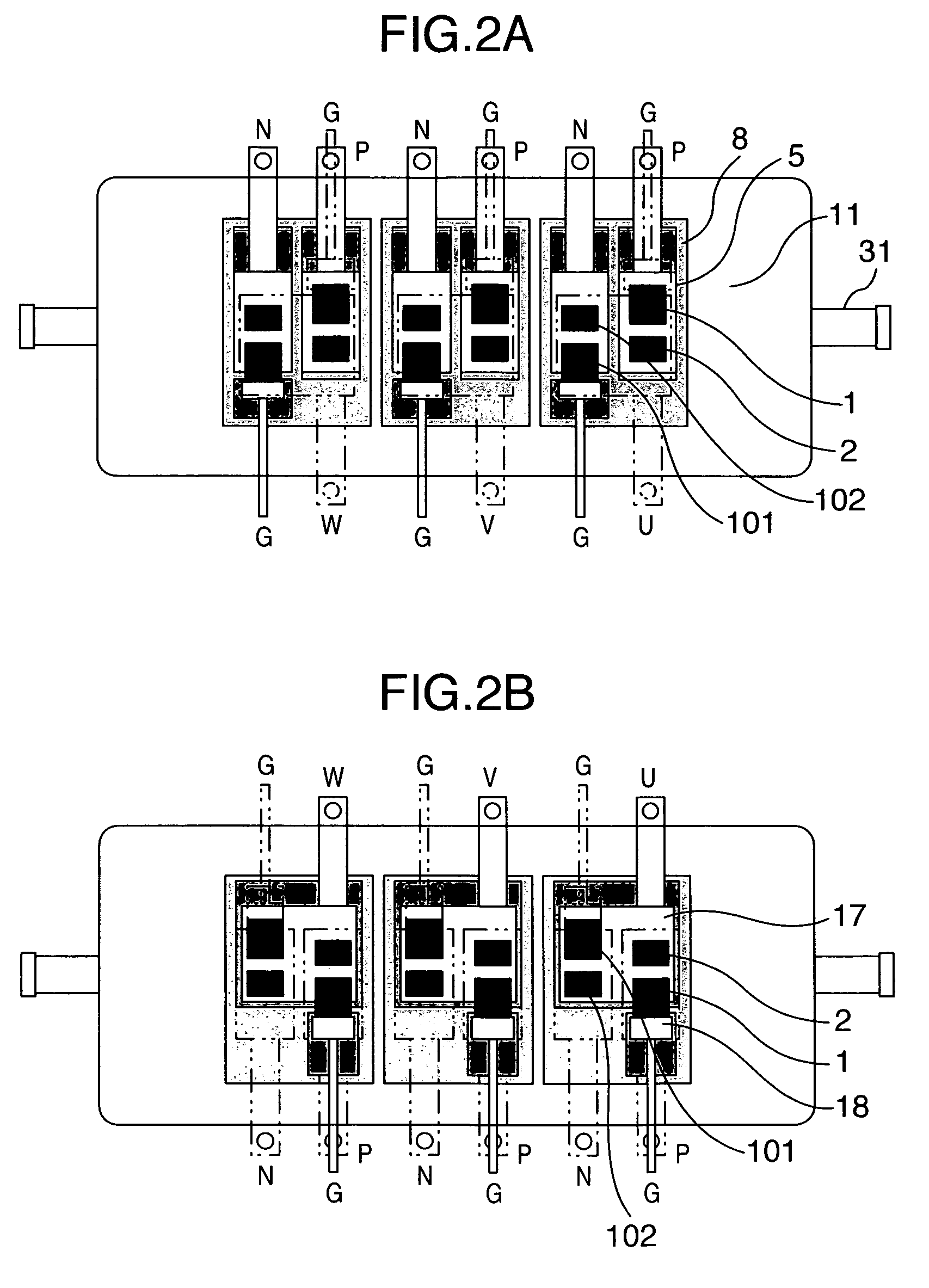
- Summary
- Abstract
- Description
- Claims
- Application Information
AI Technical Summary
Benefits of technology
Problems solved by technology
Method used
Image

Examples
embodiment 1
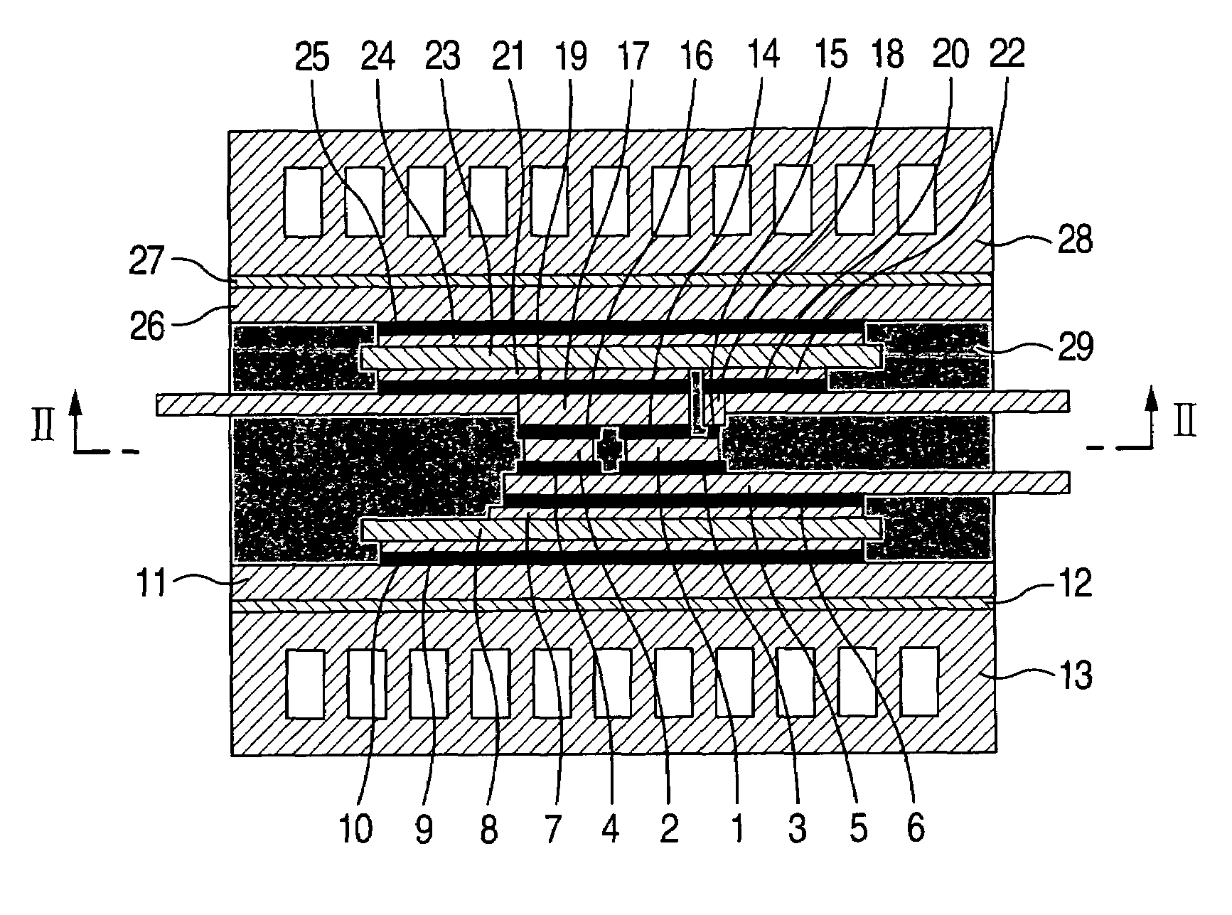
[0017]An embodiment of the present invention will be explained by referring to the drawings. FIG. 1 shows a vertical cross-sectional view of a power semiconductor module in accordance with the embodiment, and FIG. 2 shows a horizontal cross-sectional view thereof. Reference numeral 1 in FIG. 1 denotes a power semiconductor element such as an IGBT or a power MOS FET, and numeral 2 denotes a power semiconductor element such as a free-wheeling diode. The lower sides of the power semiconductor element 1 and the power semiconductor element 2 are bonded to a lower-side lead electrode 5 with first solders 3 and 4 disposed therebetween. The material of the lower-side lead electrode 5 may be made of copper. However, when the electrode material is made of a composite material (Cu—C) of copper and carbon having a small coefficient of linear expansion, a stress in the first solders 3 and 4 or in a second solder 6 caused by thermal deformation can be relaxed, thus increasing a reliability. The l...
embodiment 2
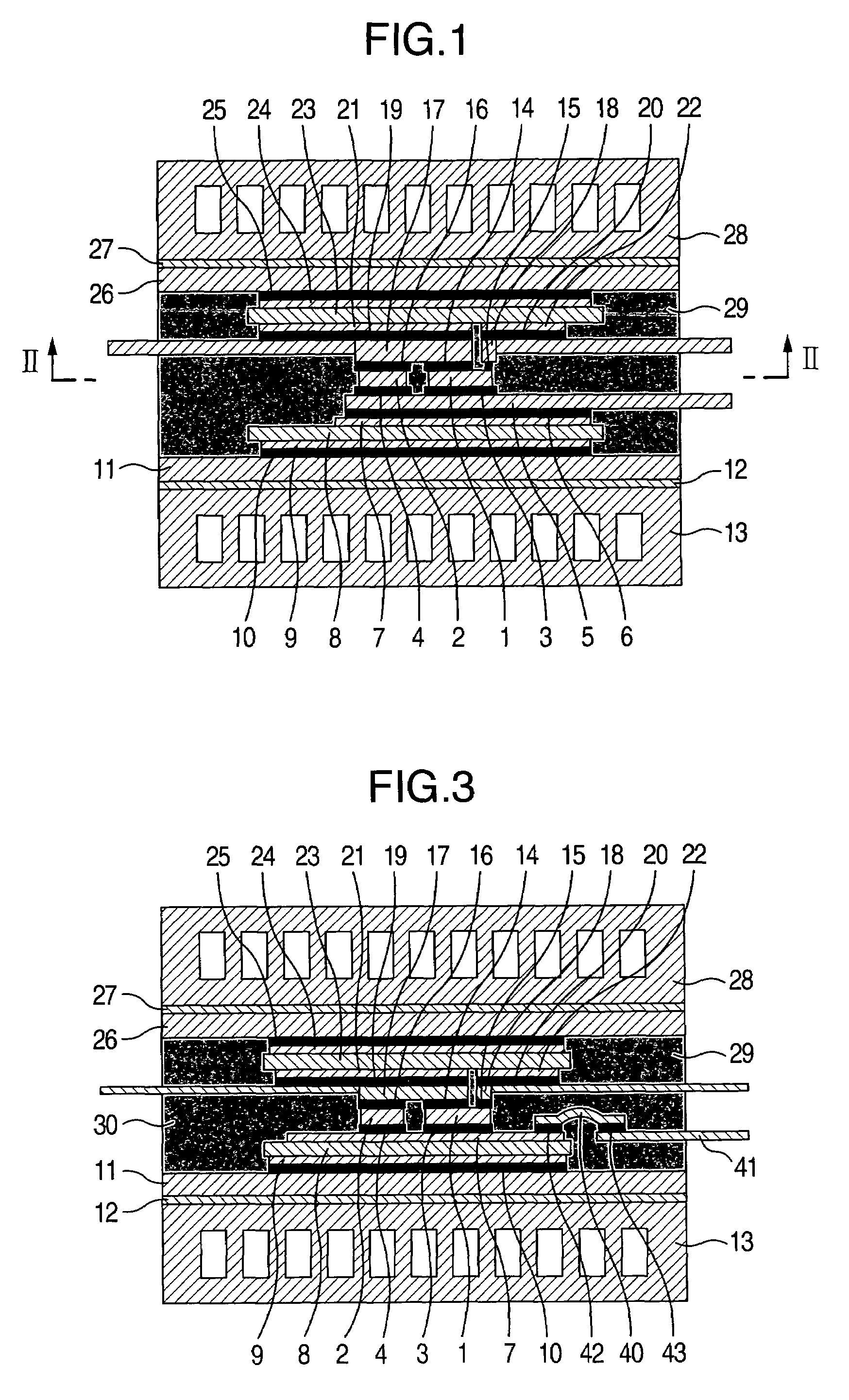
[0027]FIG. 3 shows a cross-sectional view of a power semiconductor module in accordance with this embodiment. In the present embodiment, the lower sides of the power semiconductor elements 1 and 2 are bonded to the copper foil 7 of the insulating substrate. The power semiconductor elements 1 and 2 are bonded to the copper foil 7 with the first solders 3 and 4 disposed therebetween. A plate-like connection member 40 made of copper is connected to the copper foil 7 with a solder 42 disposed therebetween, and the connection member 40 in turn is connected to an electrode terminal 41 with a solder 43 disposed therebetween. Other arrangement is similar to that in the embodiment 1 and thus explanation thereof is omitted.
[0028]As the fourth solders 14 and 15 for bonding the power semiconductor elements 1, 2 and the upper-side lead electrodes 17, 18; a high temperature solder, e.g., having copper particles and tin particles mixed therein is used. Even for the first solders 3, 4 for bonding t...
embodiment 3
[0030]FIG. 4 shows a vertical cross-sectional view of a power semiconductor module in accordance with this embodiment, and FIGS. 5A and 5B show horizontal cross-sectional views thereof. More specifically, FIG. 5A is a cross-sectional view when taken along a line V-V in FIG. 4 and viewed from its lower side, and FIG. 5B is a cross-sectional view when taken along the line V-V and viewed from its upper side. In the present embodiment, the lower sides of the power semiconductor elements 1 and 2 are bonded to the copper foil 7 of the lower-side insulating substrate. The power semiconductor elements 1 and 2 are bonded to the copper foil 7 with the first solders 3 and 4 disposed therebetween. Meanwhile, the upper sides of the power semiconductor elements 1 and 2 are bonded to the copper foils 21 and 22 bonded to the upper-side insulating substrate 23. The power semiconductor elements 1 and 2 and the copper foils 21 and 22 are bonded together with the fourth solders 14, 15, and 16. The plat...
PUM
 Abstract
Description
Claims
Application Information