Process for manufacturing an LED lamp with integrated heat sink

a technology of led lamps and heat sinks, which is applied in the direction of conductive pattern formation, semiconductor devices of light sources, lighting and heating apparatus, etc., can solve the problems of unsatisfactory resolution of high-power led technology, permanent deformation, and inability to achieve light output sensitivity, so as to maximize heat transfer from leds

Active Publication Date: 2010-03-16
THE ARTAK TER HOVHANISSIAN PATENT TRUST +1
View PDF17 Cites 49 Cited by
  • Summary
  • Abstract
  • Description
  • Claims
  • Application Information

AI Technical Summary

Benefits of technology

[0011]Circuit traces are formed on the anodized surface of the base to establish discreet and electrically conductive paths for electrically interconnecting electronic components. The circuit traces include at least one LED landing. An LED is then electrically and mechanically attached to the LED landing by means of conductive metallic solder. Thus, heat generated from the LED is transferred through the metallic solder and circuit LED landing to the thermally conductive base. Due to the fact that the solder comprises a conductive metallic material, such as a tin alloy material comprising tin and lead, copper or silver, heat transfer from the LED is maximized as it flows from the metallic LED heat sink slug to the solder and through the circuit traces and into the base.

Problems solved by technology

One aspect of high powered LED technology that has not been satisfactorily resolved is the removal of heat generated by the LED.
LED lamps exhibit a substantial light output sensitivity to temperature, and in fact are permanently degraded by excessive temperature.
However, these LEDs emit a substantial amount of heat during their operation, which can permanently degrade the LED over time, resulting in a lower output and operating life.
In ideal conditions, the life of the LED is 50,000-100,000 hours, however, this life can be shortened to less than 10% of the designed life due to the heat generated by these new super bright LEDs.
However, these arrangements have several disadvantages.
These PCBs still have thermal conductivity problems when used with high output LEDs, and do not perform well due to core thermal conductivity of the dielectric.
When the LED is attached to a standard PCB, the heat is trapped under the LED due to the low thermal conductivity of the fiberglass circuit board, insulating sheet, etc.
However, the adhesive attachment of the heat sink LEDs to the metallic heat sink in this manner, while an improvement of the other methods, still presents some disadvantages.
Thus, once again, heat can be trapped under the LED.
Other components surrounding the light emitting chip are typically plastic or silicon and not intended to transmit the heat away from the chip.
Another disadvantage is that adhesive attachment systems sometimes exhibit detachment due to repeated temperature cycles.
The relatively large differences in thermal expansion coefficients of plastics, epoxies and metals can give rise to substantial stresses of the attachment region.
These stresses may exceed the strength of the adhesive and may eventually result in joint failure.
This could result in the LED being electrically disconnected from the circuit.

Method used


Image

  • Process for manufacturing an LED lamp with integrated heat sink
  • Process for manufacturing an LED lamp with integrated heat sink
  • Process for manufacturing an LED lamp with integrated heat sink

Examples


Embodiment Construction

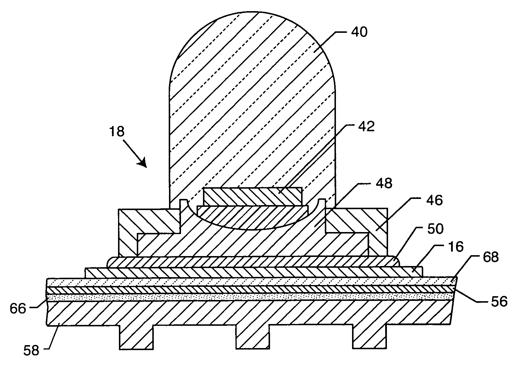
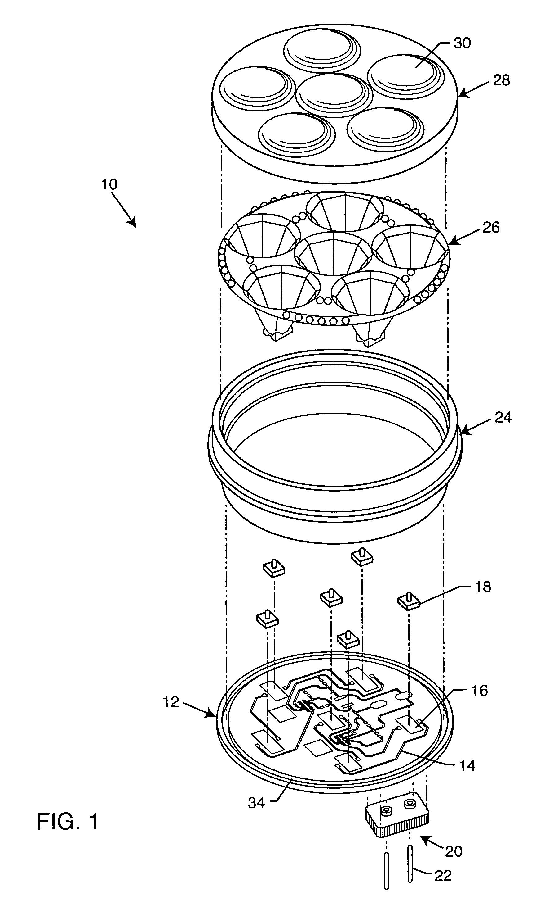
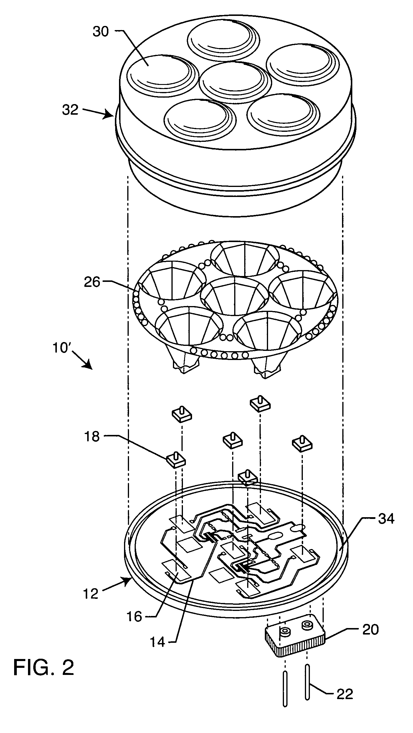
[0030]As shown, in the accompanying drawings, for purposes of illustration, the present invention resides in an LED lamp assembly, and particularly in a method for manufacturing these in such a way to remove the heat generated by the LEDs in an efficient manner. When referring to the Figures, like numerals indicate like or corresponding parts throughout several views.

[0031]With reference now to FIG. 1, an LED lamp assembly, generally referred to by the reference number 10, embodying the present invention is shown. The assembly 10 includes an electrically and thermally conductive base 12. The base 12 includes a very thin electrically insulating coating, on at least a portion of the surface thereof. Typically, the base 12 is comprised of a metal material with at least a portion of a top surface thereof anodized. For example, the base 12 is typically comprised of aluminum or an aluminum alloy.

[0032]Aluminum is a superb thermal conductor, being 90% more thermally conductive than a tradi...


PUM

PropertyMeasurementUnit
electricallyaaaaaaaaaa
thermally conductiveaaaaaaaaaa
electrically insulatingaaaaaaaaaa

Abstract

A method for manufacturing an LED lamp assembly includes anodizing at least a portion of a surface of an electrically and thermally conductive base, such as an aluminum or aluminum alloy base, so as to form an electrically insulating coating. The base may form a heat sink or be coupled to a heat sink. Circuit traces are formed on the anodized surface of the base, which include LED landings. LEDs are electrically and mechanically attached to the LED landing by a conductive metallic solder such that heat generated from the LED is transferred efficiently through the solder and circuit traces LED landings to the base and heat sink through a metal-to-metal contact pathway.

Description

BACKGROUND OF THE INVENTION[0001]The present invention generally relates to light emitting diode arrays. More particularly, the present invention relates to a light emitting diode (LED) lamp assembly manufactured in such a manner so as to have an integrated heat sink to avoid degrading temperatures otherwise created by the light emitting diodes.[0002]Light emitting diodes (LEDs) have been available since the early 1960s in various forms, and are now widely applied in a variety of ways, including signs and message boards, vehicle lights, and even interior lights. The relatively high efficiency of LEDs is the primary reason for their popularity. Tremendous power savings are possible when LEDs are used to replace traditional incandescent lamps of similar luminous output.[0003]One aspect of high powered LED technology that has not been satisfactorily resolved is the removal of heat generated by the LED. LED lamps exhibit a substantial light output sensitivity to temperature, and in fact...

Claims


Application Information

Patent Timeline
Patent Type & Authority Patents(United States)
IPC IPC(8): H05K3/34F21K99/00
CPCH05K1/0203F21V29/77F21K9/00F21Y2101/02H05K1/053H05K3/0061H05K2201/10106Y10T29/49144F21V23/06Y10S362/80Y10T29/4935Y10T29/53113Y10T29/49155H05K2203/0315F21Y2115/10
Inventor TER-HOVHANNISSIAN, ARTAK
Owner THE ARTAK TER HOVHANISSIAN PATENT TRUST
Why Eureka
Try Eureka