

Communications chip having a plurality of logic analysers
a logic analysis and communication chip technology, applied in the field of communication chips, can solve problems such as destroying signals and becoming increasingly difficult to use such a conventional logic analysis devi
- Summary
- Abstract
- Description
- Claims
- Application Information
AI Technical Summary
Benefits of technology
Problems solved by technology
Method used
Image

Examples
Embodiment Construction
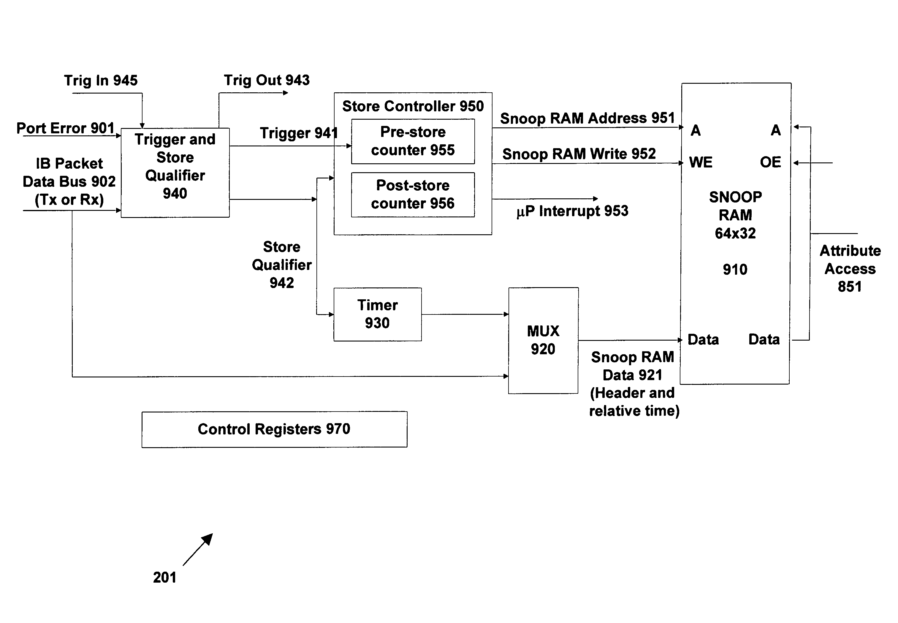
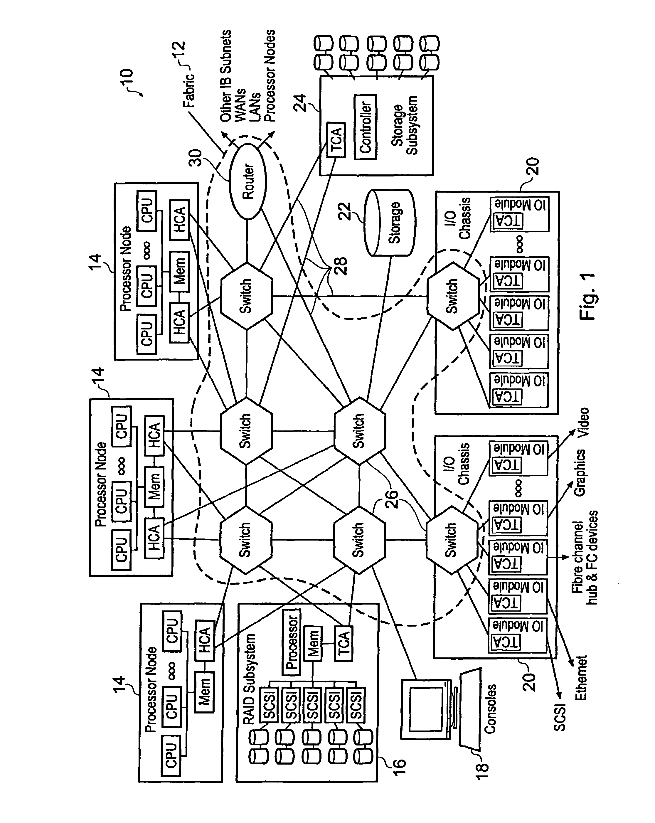
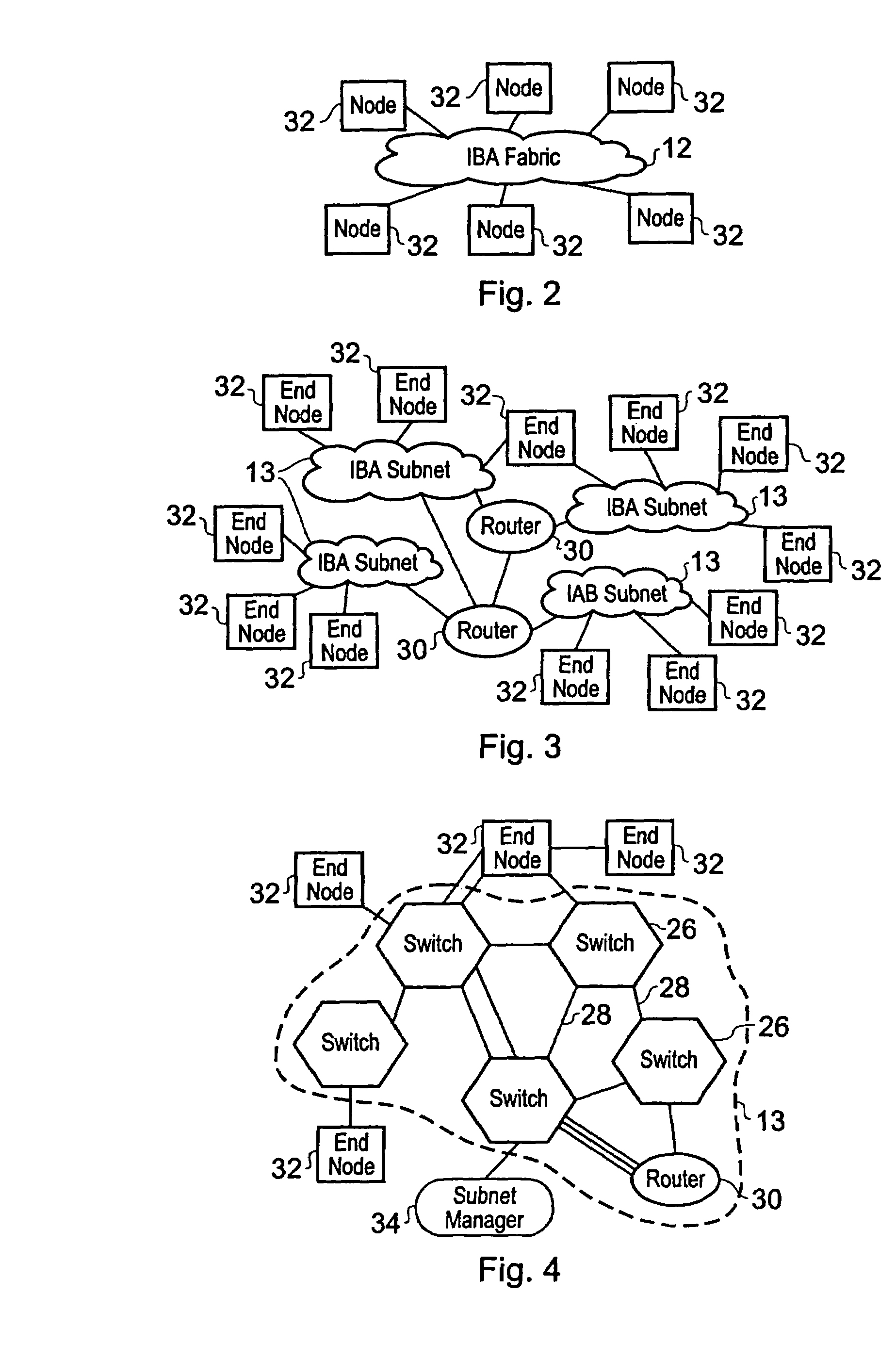
[0026]The Infiniband architecture provides a standard computer networking environment defined and administered by the Infiniband Trade Association, which was founded by Compaq, Dell, Hewlett-Packard, IBM, Intel, Microsoft and Sun Microsystems (Infiniband is a trademark of the Infiniband Trade Association; other names are trademarks of their respective companies). The Infiniband Architecture defines a System Area Network (SAN) for connecting multiple independent processor platforms (i.e., host processor nodes), I / O platforms and I / O devices. A full definition of the Infiniband Architecture may be found in the Infiniband Architecture Specification Volumes 1 and 2, available from the Infiniband Trade Association, and which is hereby incorporated by reference.
[0027]An Infiniband Architecture system area network (SAN) provides a communications and management infrastructure supporting both I / O and interprocessor communications for one or more computer systems. An Infiniband Architecture s...
PUM
 Abstract
Description
Claims
Application Information