High light efficiency solid-state light emitting structure and methods to manufacturing the same

a technology of solid-state light and structure, which is applied in the direction of semiconductor/solid-state device manufacturing, semiconductor devices, electrical devices, etc., can solve the problems of reducing the reflectivity of odr, disadvantageous structure above fig. 5, and device performance degradation, so as to enhance the reflectivity and thus the extraction efficiency of led devices. , the effect of increasing the index contrast of the reflective mirror

Active Publication Date: 2010-03-23
DICON FIBEROPTICS
View PDF29 Cites 19 Cited by
  • Summary
  • Abstract
  • Description
  • Claims
  • Application Information

AI Technical Summary

Benefits of technology

[0019]In the above embodiment, the buffer layer separates the current spreading layer from the reflective metal layer. In the event that the material of reflective metal layer reacts with that of the current spreading layer, the presence of a buffer layer reduces or prevents such reaction. This is the case, for example, where the current spreading layer comprises ITO. Moreover, since the buffer layer has a refractive index that is below that of the current spreading layer, this increases the index contrast of the reflective mirror formed by the buffer layer and the reflective metal layer, and enhances the reflectivity and thus the extraction efficiency of the LED device.

Problems solved by technology

The rest is reflected into the semiconductor where it will eventually be reabsorbed or recycled and results in the performance degradation of the device.
In section 3.3.3 on page D-9 of this paper, however, the authors Kim, et al. indicated that the above structure of FIG. 5 is disadvantageous because the above design “needs absorptive semi-transparent current spreading layer, such as RuO2, .
. . , which leads to a decrease in reflectivity of the ODR.” Furthermore, the refractive index of silicon dioxide is deemed to be not low enough for high refractive index contrast with high-index semiconductor materials, which limits further improvement of light extraction efficiency in GaN-based LEDs.
However, as illustrated in FIG. 13 of the paper, the ITO nanorod layer provides mediocre ohmic contact characteristics.
When the ITO nanorod layer proposed by Kim, et al. comes into contact with a silver substrate underneath, interdiffusion occurs at the interface which greatly reduces the reflective properties of the resulting structure.
This will also greatly reduce the light extraction efficiency of the LED.
Poor thermal management leads to performance degradation and reduced lifetime of LEDs.
Given that conventional red (AlGaInP) and blue (InGaN) LED are grown from N+ GaAs and sapphire substrates, respectively, one of the major drawbacks of GaAs and sapphire are their poor thermal conductivity.
When the growth substrate is replaced by a substitute substrate, such as one made of Si or Cu, the LED epitaxial layers may be subject to change in stress conditions, which may damage the LED.
Thus, in the case of GaN-based LEDs grown from sapphire substrates, the fabrication process introduces considerable stress on the LED.
When the sapphire substrates are replaced, the LEDs may be damaged if such stress is released rapidly.
Stress management is thus an important issue.
Since these materials are in intimate contact, this uneven expansion and contraction potentially introduce enormous stress in the LED fabricated.
Such technique, will however, limit the type of materials that can be used, which is not desirable.

Method used


Image

  • High light efficiency solid-state light emitting structure and methods to manufacturing the same
  • High light efficiency solid-state light emitting structure and methods to manufacturing the same
  • High light efficiency solid-state light emitting structure and methods to manufacturing the same

Examples


Embodiment Construction

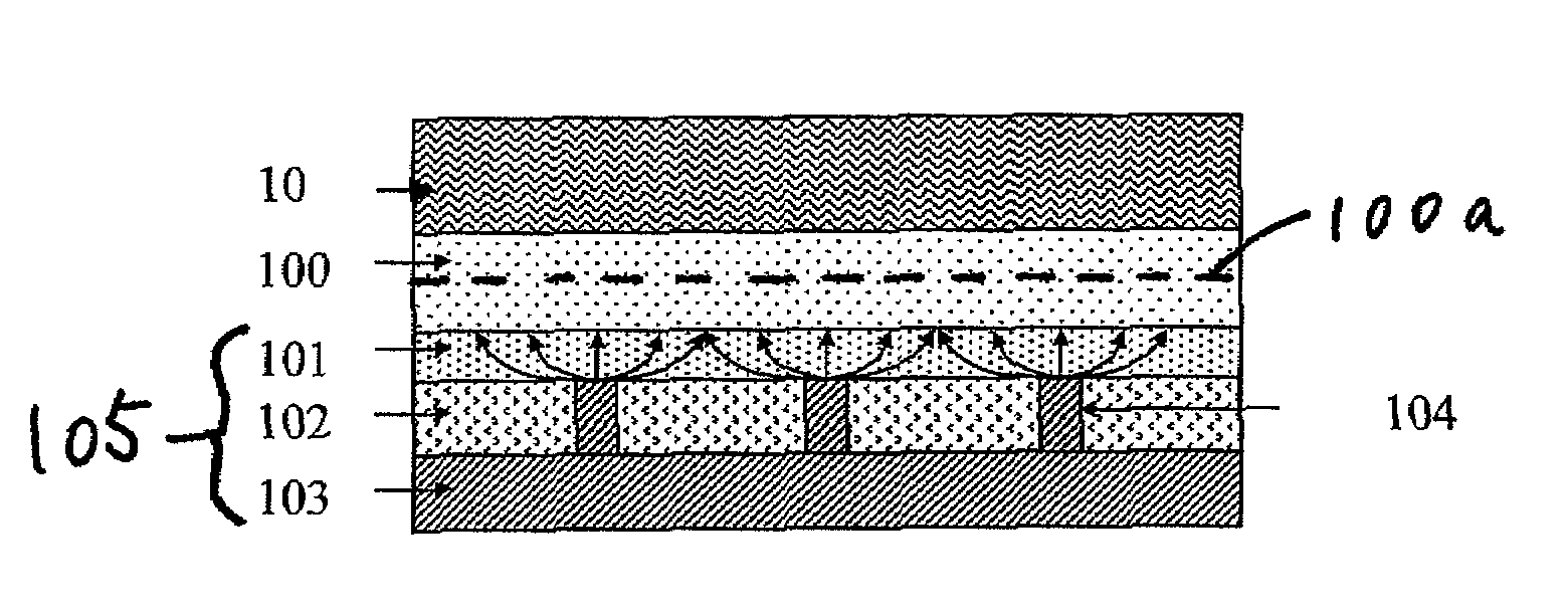
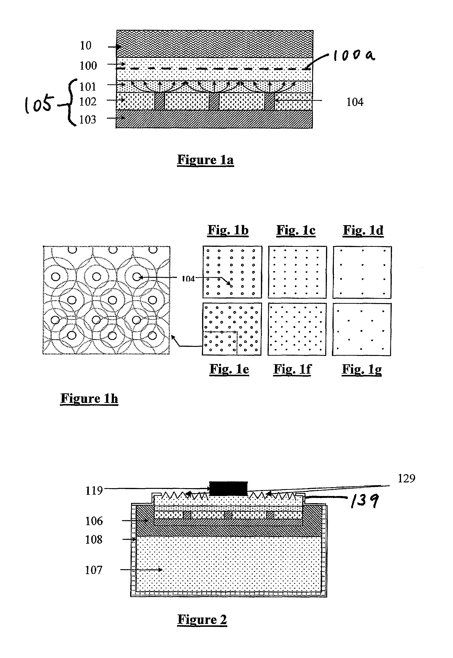
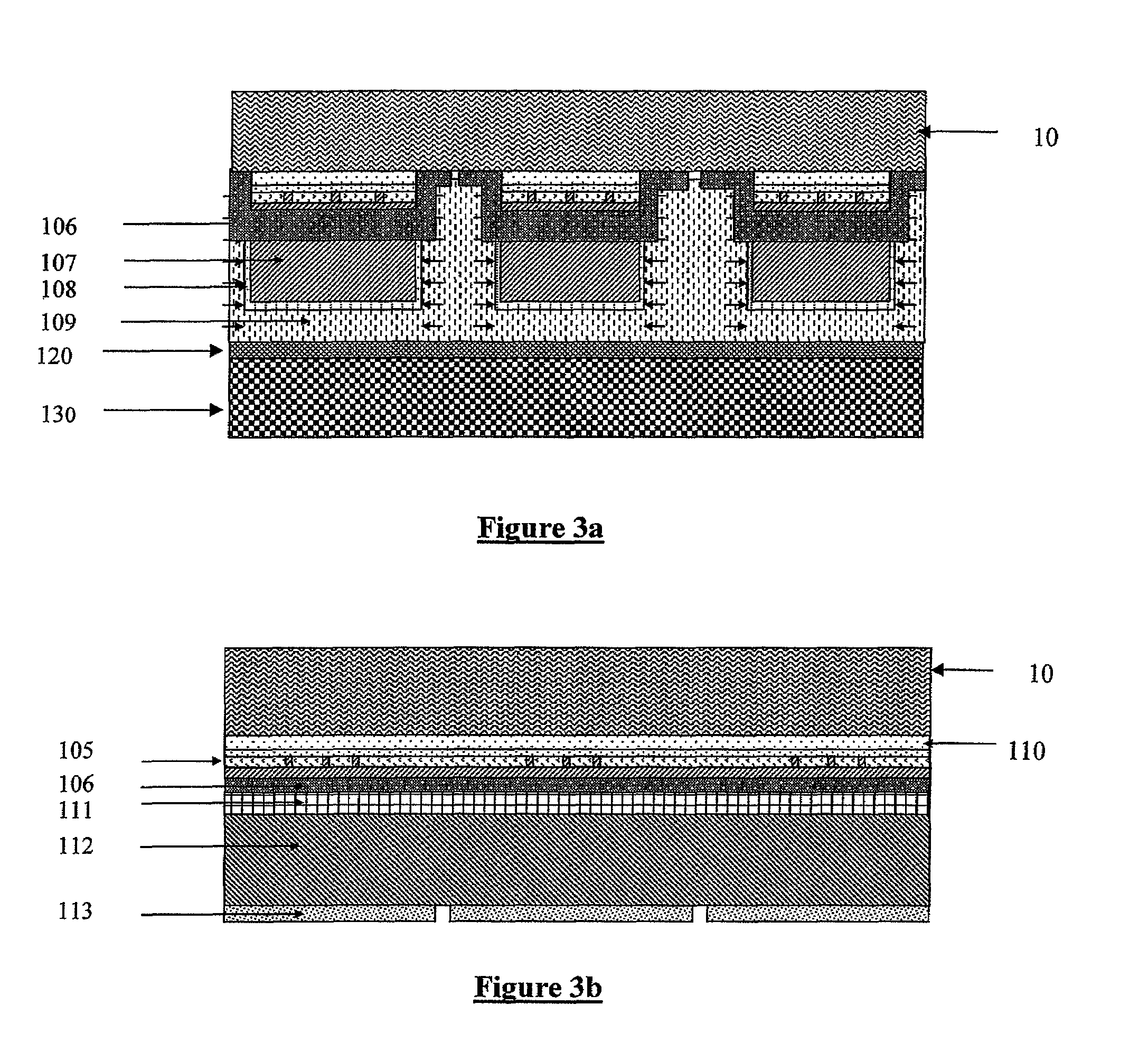
[0039]In some of the embodiments of the present invention, a light emitting structure is provided with high light extraction efficiency, as well as high thermal dissipation properties. The structure and manufacturing processes provide three major advantages when compared to existing structures and manufacturing methods:[0040]1. A Composite Reflective Mirror is used to enhance the light extraction efficiency and total brightness output of the light-emitting device.[0041]2. An innovative method is used to manage physical or mechanical stresses within the die structure. The light-emitting material is supported by a new substrate that has a different CTE than the active epi-layers of the device (i.e., the layers of the device that are grown using an epitaxial growth process). The substrate that supports the epi-layers is designed to provide robust mechanical support to the epi-layers as well as high thermal conductivity. This is accomplished by using a substrate or carrier material that...


PUM


Abstract

In one embodiment of an epitaxial LED device, a buffer layer (e.g. dielectric layer) between the current spreading layer and the substitute substrate includes a plurality of vias and has a refractive index that is below that of the current spreading layer. A reflective metal layer between the buffer layer and the substitute substrate is connected to the current spreading layer through the vias in the buffer layer. The buffer layer separates the current spreading layer from the reflective metal layer. In yet another embodiment, stress management is provided by causing or preserving stress, such as compressive stress, in the LED so that stress in the LED is reduced when it experiences thermal cycles. In one implementation of this embodiment, a layer is attached to the LED and reflective metal layer, and causes or preserves stress in the LED along one or more directions parallel to an interface between the LED epitaxial layers so that stress in the LED is reduced in said one or more directions when temperature of the structure is increased.

Description

CROSS REFERENCE TO RELATED APPLICATION[0001]This patent application claims the benefit of U.S. provisional patent application No. 60 / 937,245 entitled “High Light Efficiency Solid-State Light Emitting Structure And Methods To Manufacturing The Same”, filed on Jun. 25, 2007.BACKGROUND OF THE INVENTION[0002]Over the last decade, the advent of solid-state lighting has led to rapid advances in the production of high brightness Light Emitting Diodes (LEDs). LEDs hold the promise for a cost-effective solution for ever-increasing illumination-related energy needs. With advanced LED technology, the energy consumption can be reduced significantly.[0003]LEDs brightness is now competing with incandescent and fluorescent light sources: larger chip-size and higher drive-current are keys to the latest improvements. Core-Technological breakthroughs, as well the innovative implementation of optical, electrical and thermal management methods have made these possible. Two aspects of these breakthrough...

Claims


Application Information

Patent Timeline
Patent Type & Authority Patents(United States)
IPC IPC(8): H01L27/15H01L29/06H01L29/22H01L29/227H01L29/26H01L31/0328H01L31/0336H01L31/072H01L31/109H01L31/12H01L33/00H01L33/14H01L33/38H01L33/40
CPCH01L33/0079H01L33/387H01L33/405H01L33/14H01L33/22H01L2224/48247H01L2224/48091H01L2924/00014H01L33/0093
Inventor LEE, CHENG TSINDU, QINGHONGNAULIN, JEAN-YVES
Owner DICON FIBEROPTICS
Why Eureka
Try Eureka