Manufacturing method of a printed matter and a printed matter
a printing matter and manufacturing method technology, applied in the field of printed matter, can solve the problems of short circuit, low power consumption, and fast response speed, and achieve the effect of printing that accuracy is preferable and the yield of printing matter is preferabl
- Summary
- Abstract
- Description
- Claims
- Application Information
AI Technical Summary
Benefits of technology
Problems solved by technology
Method used
Image
Examples
example 1
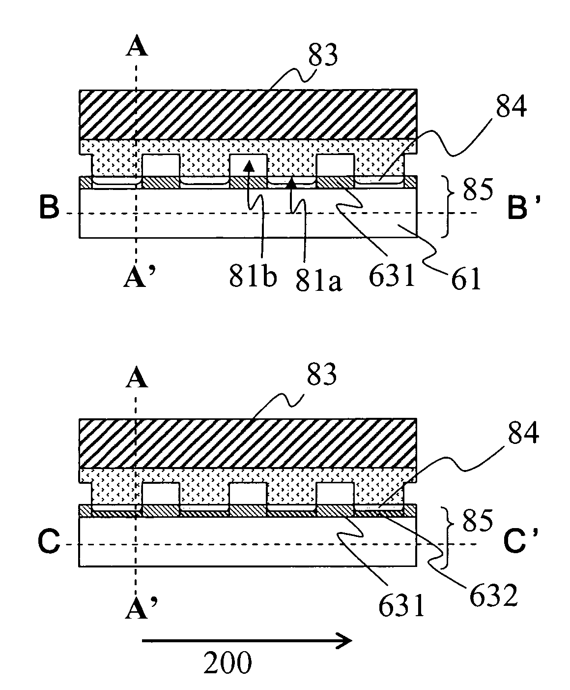
[0167]One embodiment of the invention is explained in FIG. 6 and FIG. 7.
[0168]A glass substrate of 10 cm square was used as substrate 61. It was decided that one side of this substrate 61 was the first straight line 100. It was decided that the side which was perpendicular to the first straight line 100 was the second straight line 200 (FIG. 6A).
[0169]As first electrode 62, sixty-four ITO stripe patterns which were parallel to the second straight line 200 were formed on this substrate 61 (FIG. 6B).
[0170]In addition, the figure is simplified, and only eight first electrodes are shown.
[0171]The SiO2 film of which thickness was 0.5 μm was formed on substrate 61 by CVD method. Apertures corresponding to light emitting areas were formed by dry etching method. The inorganic partition wall of which configuration was a grating was formed in this way.
[0172]This inorganic partition wall consists of the second partition wall 632 and the first partition wall lower part 631a. The second partitio...
example 2
[0196]Substrate was prepared same as example 1. Inorganic partition wall was not formed. By slit coat method same as example 1, the photosensitivity polyimide resin of which thickness was 1.2 μm was formed. By exposure / development, apertures corresponding to light emitting areas were formed. Organic partition wall of lattice shape was formed.
[0197]This organic partition wall includes the second partition wall which covers an end of the first electrode formed earlier and is parallel to the second straight line, and the first partition wall which is form of sixty-five lines and crosses over the first electrode.
[0198]The width of the first partition wall and the second partition wall was 40 μm equally.
[0199]Same as example 1, after surface treatment of the first electrode by O2 plasma treatment was performed, liquid-repellent processing of the first partition wall upper part comprising organic materials was performed.
[0200]Macromolecule hole transport material ink adjusted same as exam...
example 3
[0207]The first partition wall and the second partition wall of which heights were 1 μm were formed on substrate same as example 2. The width of the second partition wall was 20 μm. The width of the first partition wall was 40 μm.
[0208]Afterwards liquid-repellent processing and the like was performed same as example 1. And organic luminescence media layer was formed same as example 1. Printing area of relief printing plate got over the second partition wall. And printing was performed.
[0209]The second partition wall was narrower in comparison with the first partition wall. Therefore, influence of the second partition wall on printing plate was small. Therefore, distance between printing plate and substrate could be shortened. Therefore, the phenomenon that ink remained on printing plate was able to be controlled.
[0210]In addition, ink on printing plate was cut by means of the second partition wall naturally. Therefore, ink did not remain on partition wall.
[0211]Second electrode was ...
PUM
 Abstract
Description
Claims
Application Information


