Semiconductor radiation detector

a radiation detector and semiconductor technology, applied in the field of radiation detection, can solve the problems of polycrystalline ingots with twins, inclusions, grain boundary defects, and one or more drawbacks regarding their use,

a radiation detector and semiconductor technology, applied in the field of radiation detection, can solve the problems of polycrystalline ingots with twins, inclusions, grain boundary defects, and one or more drawbacks regarding their use,

US7687780B2Inactive Publication Date: 2010-03-30BABCOCK & WILCOX TECH SERVICES Y-12 LLC +1

Image

  • Semiconductor radiation detector
  • Semiconductor radiation detector
  • Semiconductor radiation detector

Examples


Embodiment Construction

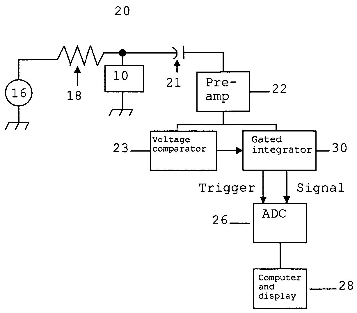
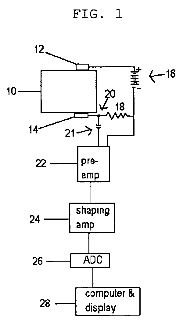
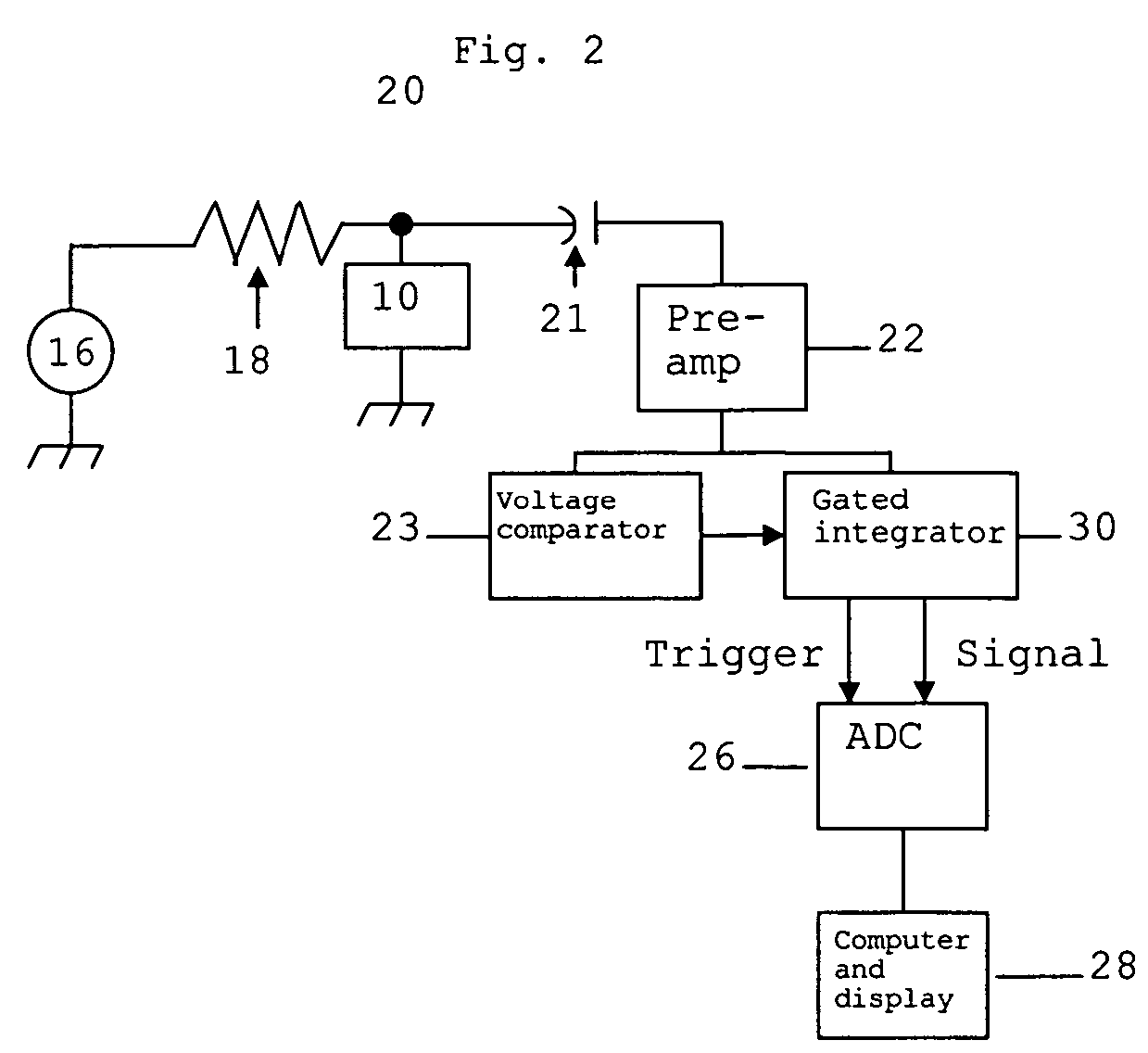
[0011]The detecting element is comprised of a compound having the composition I-III-VI2 or II-IV-V2 where the “I” component is from column 1A or 1B of the periodic table, the “II” component is from column 2B, the “III” component is from column 3A, the “IV” component is from column 4A, the “V” component is from column 5A, and the “VI” component is from column 6A. A more concise manner of description is that the crystal is formed from elements in the group of 1A-3A-6A, 1B-3A-6A or 2B-4A-5A of the periodic chart. An example from group 1A-3A-6A is Lithium-Gallium-Selenium. An example from group 1B-3A-6A is Copper-Gallium-Selenium. An example from group 2B-4A-5A is Cadmium-Germanium-Antimony. Crystals formed from groups 1B-3A-6A and 2B-4A-5A are chalcopyrites. The detecting element detects ionizing radiation by generating a signal proportional to the energy deposited in the element, and detects neutrons by virtue of the ionizing radiation emitted by one or more constituent materials subs...


PUM


Abstract

A semiconductor detector for ionizing electromagnetic radiation, neutrons, and energetic charged particles. The detecting element is comprised of a compound having the composition I-III-VI2 or II-IV-V2 where the “I” component is from column 1A or 1B of the periodic table, the “II” component is from column 2B, the “III” component is from column 3A, the “IV” component is from column 4A, the “V” component is from column 5A, and the “VI” component is from column 6A. The detecting element detects ionizing radiation by generating a signal proportional to the energy deposited in the element, and detects neutrons by virtue of the ionizing radiation emitted by one or more of the constituent materials subsequent to capture. The detector may contain more than one neutron-sensitive component.

Description

GOVERNMENT RIGHTS[0001]The U.S. Government has rights to this invention pursuant to contract number DE-AC05-00OR22800 between the U.S. Department of Energy and Babcock & Wilcox Technical Services.BACKGROUND OF THE INVENTION[0002]1. Field of the Invention[0003]The invention is generally related to radiation detection and more particularly to a semiconductor detector of ionizing electromagnetic radiation, neutrons, and energetic charged particles.[0004]2. General Background[0005]The present state of the art in semiconductor radiation detection is silicon diodes, high purity germanium (cooled by liquid nitrogen), and compound semiconductors such as cadmium zinc telluride (CZT), and mercuric iodide. Each of these materials has one or more drawbacks regarding its use. Silicon has a low atomic number and is therefore primarily useful for the detection of charged particles and atomic x rays emitted from low atomic number elements. Germanium has a higher atomic number but, because of its lo...

Claims


Application Information

Patent Timeline
30 Mar 2010
Publication
US7687780B2
IPC
G01T1/16
CPC
G01T1/24; G01T3/08
Inventors
BELL, ZANE W.; BURGER, ARNOLD