
Yttrium contacts for germanium semiconductor radiation detectors

a technology of germanium semiconductor and radiation detector, applied in the field of radiation detectors, can solve the problems of affecting the use of germanium semiconductor radiation detectors, unable to reach the 1000 thickness level required for a truly thin particle entrance window, and lithium diffused contacts, so as to improve the contact technology of germanium detectors, improve the effect of germanium detectors, and convenient segmentation

Active Publication Date: 2011-12-08
HULL ETHAN +3
View PDF3 Cites 10 Cited by
  • Summary
  • Abstract
  • Description
  • Claims
  • Application Information

AI Technical Summary

Benefits of technology

[0010]An object of the invention is to provide improved germanium-detector contact technology for the hole-barriers or positively biased contacts on germanium semiconductor radiation detectors. In particular, an object of the invention is to provide a thin hole-barrier contact that can be conveniently segmented. An additional object of the invention is a contact technology that can also serve as reasonable electron-barrier contacts thereby allowing both polarity contacts to be fabricated using the same processes. Yttrium metal forms excellent thin hole-barrier contacts when deposited onto germanium. Yttrium metal also forms reasonable electron-barrier contacts when deposited onto germanium. Yttrium contacts can be conveniently segmented into an arbitrary number of electronically independent contact segments conveniently using ordinary semiconductor photolithography. When germanium detectors with yttrium contacts are cooled to the liquid nitrogen temperature range, the yttrium contact immediately demonstrates the formation of the historically elusive hole-barrier contact capable of withstanding reasonably high electric fields. The yttrium contact also provides a reasonable electron-barrier contact. In addition, the thin yttrium layer provides a sufficiently good metallic connection to the active volume of the germanium detector to facilitate excellent gamma-ray spectroscopy.

Problems solved by technology

Historically, the use of germanium semiconductor radiation detectors has been adversely affected by the lack of a convenient thin hole-barrier contact to serve opposite these thin electron-barrier contacts.
Although lithium contacts can be made less thick, they cannot approach the 1000 Å thickness level required for a truly thin particle entrance window.
Although extremely rugged, reliance upon thick lithium diffused contacts has greatly limited the use of germanium detectors as transmission detectors in charged-particle telescopes for nuclear physics experiments.
In addition, lithium diffused contacts prohibit the transmission of low energy photons for low energy photon spectroscopy.
However, the inherent thickness of the lithium diffused layer presents a significant limitation to the segmentation feature sizes possible.
However, fabrication of the phosphorus implanted n+ contact is an extremely involved process requiring high temperature annealing steps that can significantly harm the charge collection properties of the germanium crystal.
Despite great effort, phosphorus contacts have not consistently supported the high electric fields needed for optimum charge collection.
Unfortunately, amorphous semiconductor contacts are not as stable or repeatable as desired.
Amorphous germanium contacts do not always form sufficiently high charge injection barriers to prevent significant leakage current at higher temperatures (˜95 K).

Method used


Image

  • Yttrium contacts for germanium semiconductor radiation detectors
  • Yttrium contacts for germanium semiconductor radiation detectors
  • Yttrium contacts for germanium semiconductor radiation detectors

Examples


Embodiment Construction

[0015]For illustrative purposes, a representative embodiment of the invention is described hereinafter in the context of a radiation detector. It will be understood, of course, that the utility of the yttrium metal contact on germanium detectors is not limited to the representative embodiment described specifically but extends quite readily to all germanium semiconductor detector embodiments used for a wide variety of applications including, but not limited to, x-ray detection, gamma-ray detection, charged particle detection, gamma-ray imaging, and other fields where a thin germanium detector contact or a contact that can be segmented into multiple electrodes is preferred. This is quite apparent as all germanium semiconductor radiation detectors operated in single-photon counting mode utilize detector contacts to serve as hole-barrier contacts, electron-barrier contacts, or both hole- and electron-barrier contacts. It is impossible to operate such a germanium semiconductor detector ...


PUM


Abstract

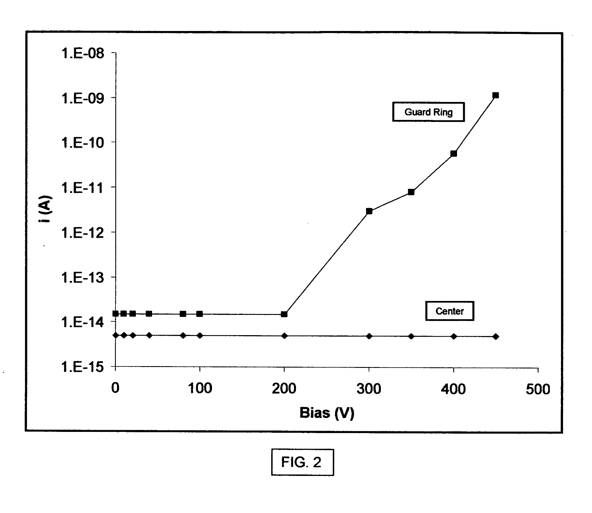
A germanium semiconductor radiation detector contact made of yttrium metal. A thin (˜1000 Å) deposited layer of yttrium metal forms a thin hole-barrier and / or electron-barrier contact on both p- and n-type germanium semiconductor radiation detectors. Yttrium contacts provide a sufficiently high hole barrier to prevent measurable contact leakage current below ˜120 K. The yttrium contacts can be conveniently segmented into multiple electrically independent electrodes having inter-electrode resistances greater than 10 GΩ. Germanium semiconductor radiation detector diodes fabricated with yttrium contacts provide good gamma-ray spectroscopy data.

Description

[0001]This nonprovisional patent application corresponds to provisional patent application No. 61 / 397,141 having a filing date of Jun. 8, 2010 and confirmation number 1363.STATEMENT REGARDING FEDERALLY SPONSORED RESEARCH OR DEVELOPMENT[0002]This invention was made with government support under DE-SC0002477 awarded by the U.S. Department of Energy Office of Nuclear Physics. The government has certain rights in the invention.CROSS REFERENCE TO RELATED APPLICATIONS[0003]Not ApplicableREFERENCE TO SEQUENCE LISTING, A TABLE, OR A COMPUTER PROGRAM LISTING COMPACT DISC APPENDIX[0004]Not ApplicableBACKGROUND OF THE INVENTION[0005]This invention relates to radiation detectors and, more particularly, to germanium semiconductor radiation detectors also referred to as high-purity germanium detectors.[0006]This invention has been publicly disclosed in the peer reviewed journal article: Hull E L, R. H. Pehl, J. R. Lathrop, B. S. Suttle, “Yttrium hole-barrier contacts for germanium semiconductor d...

Claims


Application Information

Patent Timeline
IPC IPC(8): H01L23/48
CPCG01T1/24G01T1/241
Inventor HULL, ETHANPEHL, RICHARDSUTTLE, BRUCELATHROP, JAMES
Owner HULL ETHAN
Learn More