Display device including an insulating layer with an opening

a technology of insulating layer and display device, which is applied in the direction of discharge tube luminescnet screen, discharge tube/lamp details, electric discharge lamps, etc., to achieve the effect of preventing deterioration of transistor characteristics for switching light emitting elements or supplying current, preventing deterioration of transistor characteristics due to light leakage from light emitting layer, and preventing deterioration of transistor characteristics

Inactive Publication Date: 2010-04-06
SEMICON ENERGY LAB CO LTD
View PDF11 Cites 36 Cited by
  • Summary
  • Abstract
  • Description
  • Claims
  • Application Information

AI Technical Summary

Benefits of technology

[0007]In view of the above problems, it is an object of the present invention to provide a display device that can display high-definition images by absorbing stray light from light generated in a light emitting layer so as to suppress negative effects due to the stray light, for example, an indistinct outline of a light emitting region corresponding to one pixel.

Problems solved by technology

Accordingly, an outline of a light emitting region corresponding to one pixel becomes indistinct since stray light is caused and light leakage is caused with respect to a non-light emitting region from the light emitting region corresponding to one pixel or characteristics of a transistor is deteriorated due to leakage of light into an active layer (a semiconductor layer) of the transistor, which results in problems.
Further, the above problems are caused in not only the bottom emission type light emitting display device, but also a so-called dual emission type display device, in which light is emitted through both a top and bottom faces of a light emitting layer.

Method used


Image

  • Display device including an insulating layer with an opening
  • Display device including an insulating layer with an opening
  • Display device including an insulating layer with an opening

Examples


embodiment mode 1

[Embodiment Mode 1]

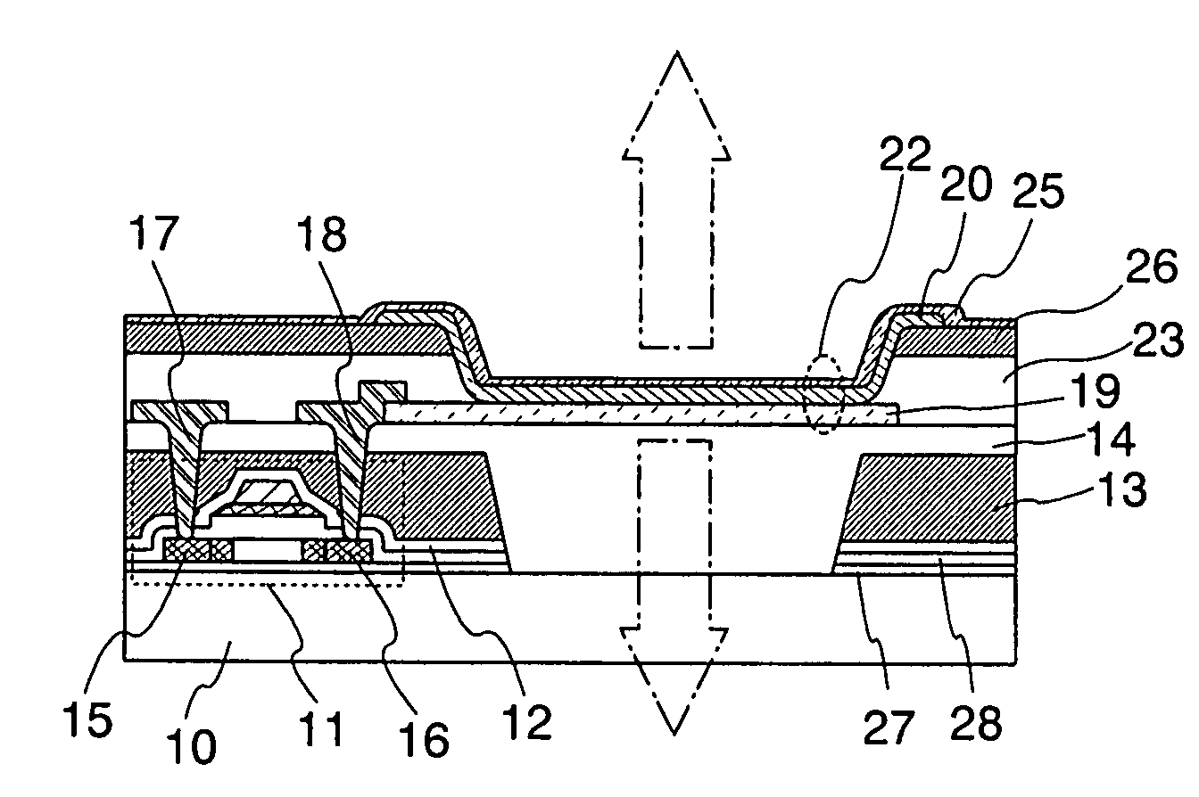
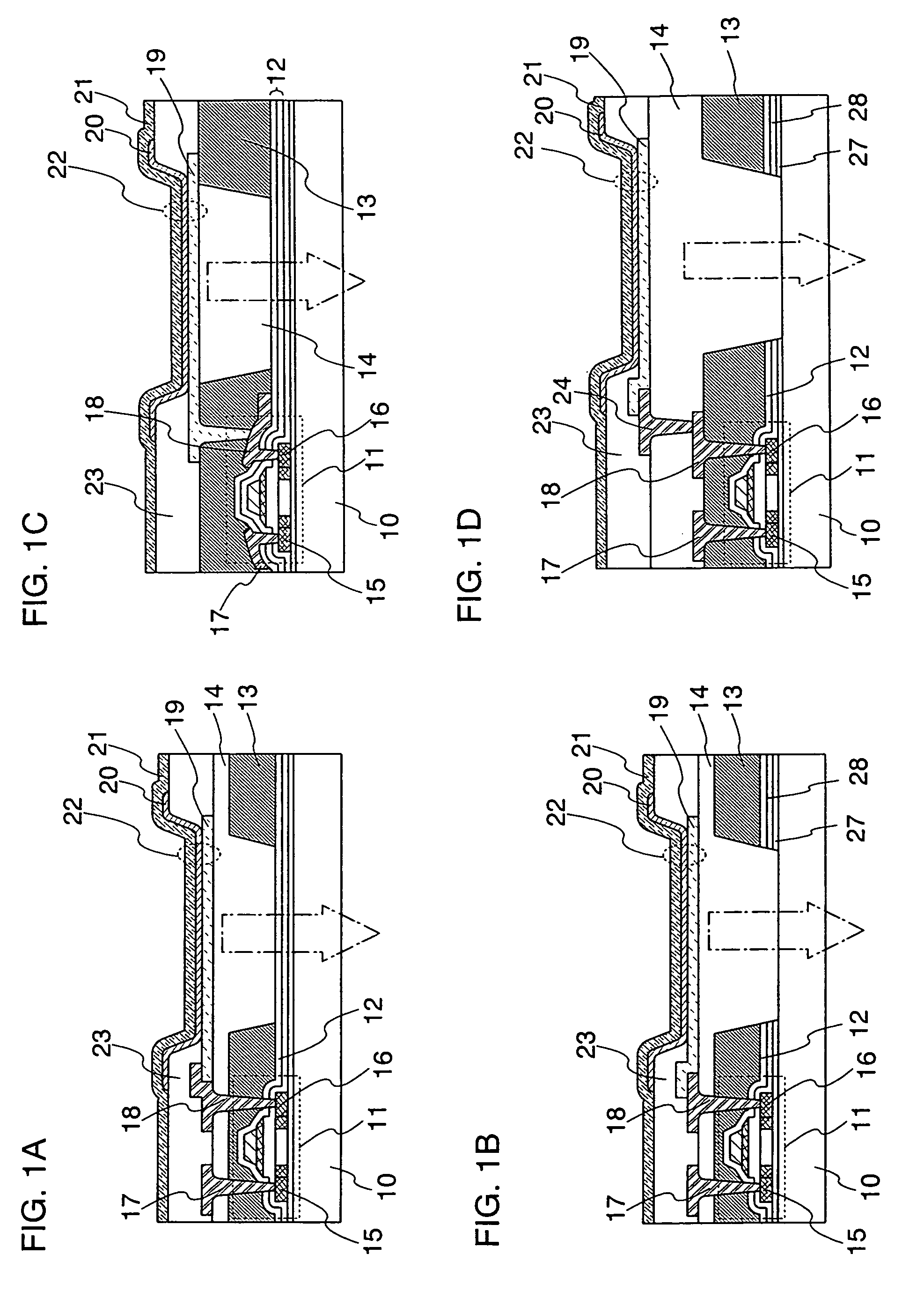
[0033]Cross sectional structures of bottom emission type display devices according to the invention, which are roughly classified into four cases, will be described with reference to the accompanying drawings. Further, in this embodiment mode, although a first insulating film 12 having a barrier property formed on a transistor is preferably formed as much as possible, it can be omitted. When the first insulating film 12 is omitted in one aspect of the invention, “a second insulating film 13” and “a third insulating film 14” as described later should be put into “a first insulating film 13” and “a second insulating film 14”, arbitrarily.

[0034]A display device of a first structure comprises a transistor 11 including a source and drain regions 15 and 16 that is formed over a substrate 10, a first insulating film 12 formed on the transistor 11, a second insulating film 13 with a light shielding property formed on the first insulating film 12, a first opening for trans...

embodiment mode 2

[Embodiment Mode 2]

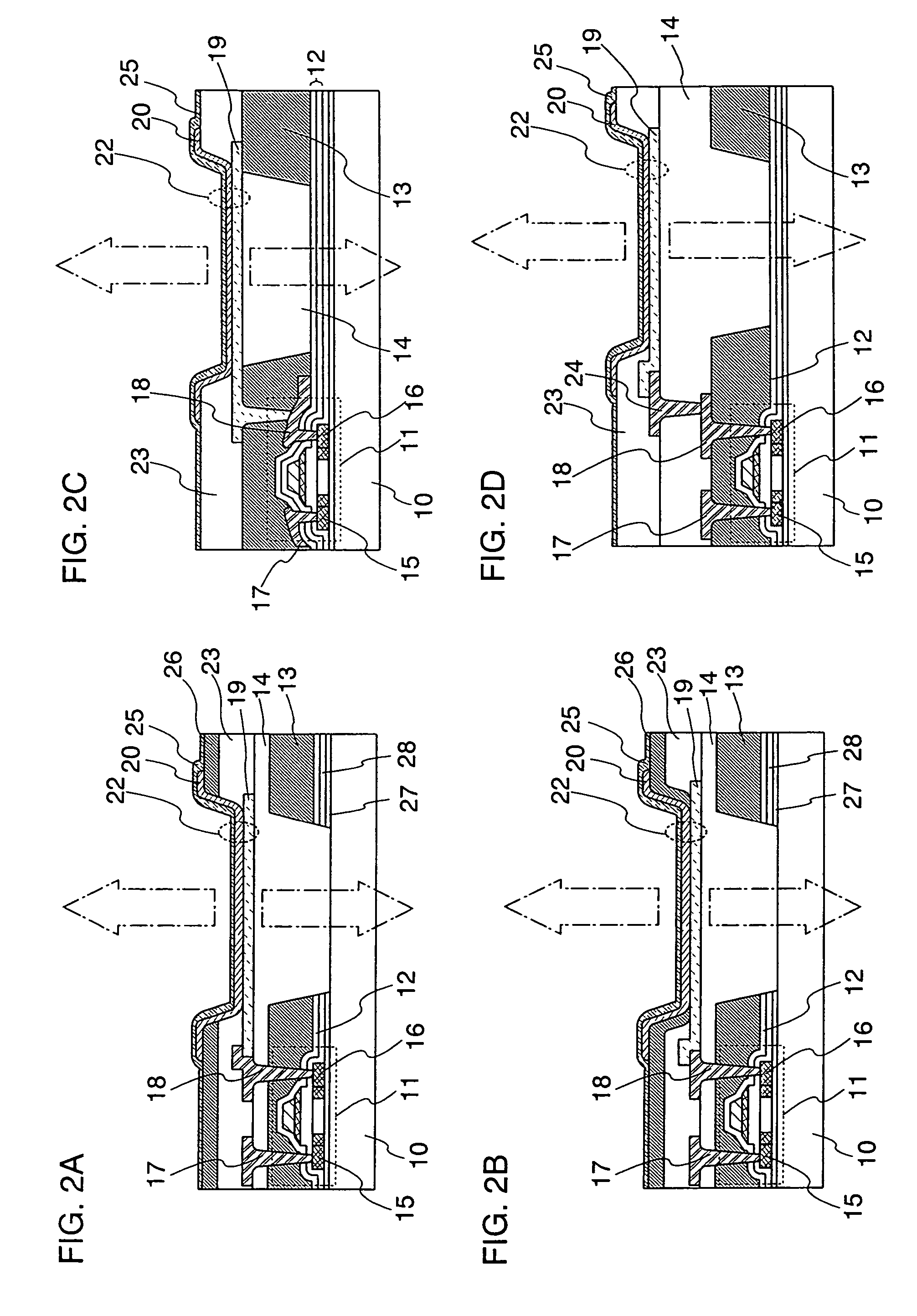
[0066]Cross sectional structures of dual emission type display devices according to the invention, which are roughly classified into four cases, will be described with reference to the drawings. Further, in this embodiment mode, although a first insulating film 12 having a barrier property formed on a transistor is preferably formed as much as possible, it can be omitted. When the first insulating film 12 is omitted in one aspect of the invention, “a second insulating film 13” and “a third insulating film 14” as described later should be put into “a first insulating film 13” and “a second insulating film 14”, arbitrarily.

[0067]A display device of a fifth structure comprises a transistor 11 formed over a substrate 10; a first insulating film 12 formed on the transistor 11; a second insulating film 13 with a light shielding property formed on the first insulating film 12; a first opening for transmitting light that is provided in the second insulating film 13; a thi...

embodiment 1

[Embodiment 1]

[0100]A structure of a display device according to the invention will be described with reference to FIGS. 3A and 3B. A display device of the invention comprises a plurality of pixels 310 each includes a plurality of elements in a region where a source line Sx (x is a natural number, which satisfies 1≦x≦m) intersects with a gate line Gy (y is a natural number, which satisfies 1≦y≦n) through an insulating material (see FIG. 3A). Each pixel 310 includes a light emitting element 313, a capacitor element 316 and two transistors. One of the two transistors is a switching transistor 311 for controlling input of a video signal to the pixel 310 while the other one is a driving transistor 312 for controlling switching ON / OFF of the light emitting element 313. The capacitor element 316 has a function of holding a gate-source voltage of the transistor 312. Further, the capacitor element 316 can be eliminated. More specifically, a gate capacitance of the transistor 312 can substit...


PUM


Abstract

When light generated in a light emitting layer of a display device is emitted through insulating films such as a planarizing film, an interlayer insulating film and a gate insulating film of a transistor, diffused reflection is caused due to slight-rough surfaces of the insulating films every time light passes through each insulating film. Accordingly, problems are caused in which stray light is caused, an outline of a pixel becomes indistinct, and a characteristic of the transistor is deteriorated. A display device according to the invention includes a transistor formed over a substrate, an insulating film with a light shielding property formed on the transistor, an opening for transmitting light therethrough formed in the insulating film with the light shielding property, and a light emitting element formed overlapping the opening.

Description

BACKGROUND OF THE INVENTION[0001]1. Field of the Invention[0002]The present invention relates to a display device having a light emitting element.[0003]2. Description of the Related Art[0004]In recent years, development of a display device having a light emitting element typified by an EL (electroluminescence) element (in particular, an organic EL element) has been carried out. By utilizing benefits of high image quality, wide viewing angle, thin shape, lightweight, etc. due to self-light emitting type, widespread application of the display device having the light emitting element has been expected. The light emitting element includes a structure formed by laminating an anode, a light emitting layer and a cathode over a substrate. For example, when an anode is formed at the side of a substrate, a so-called bottom emission type display device, in which the anode is transparent and light generated from a light emitting layer is emitted toward the substrate, is known (see patent docume...

Claims


Application Information

Patent Timeline
Patent Type & Authority Patents(United States)
IPC IPC(8): H01J1/62H01L27/32H01L51/52H05B33/00H05B33/22H05B44/00
CPCH01L51/5284H01L27/3244H10K59/12H10K50/865
Inventor YAMAZAKI, SHUNPEI
Owner SEMICON ENERGY LAB CO LTD
Why Eureka
Try Eureka