Flash memory devices that utilize age-based verify voltages to increase data reliability and methods of operating same

a flash memory and verify voltage technology, applied in the field of nonvolatile memory devices, can solve the problems of affecting the accuracy of data states or the disadvantages of flash memories to high-density integration, and achieve the effect of improving the reliability of flash memory cells, reducing the accuracy of data states or data reliability, and reducing the accuracy of data sta

Active Publication Date: 2010-04-06
SAMSUNG ELECTRONICS CO LTD
View PDF20 Cites 35 Cited by
  • Summary
  • Abstract
  • Description
  • Claims
  • Application Information

AI Technical Summary

Problems solved by technology

In general, NOR flash memories may be disadvantageous to high-density integration because of large current consumption, but advantageous to high-frequency operations.
Once one or more blocks have been worn out, functional degradation occurs.
This detrapping effect may proceed so rapidly that the accuracy of the data states or the reliability of the flash memory cell may be severely degraded.
Moreover, since the window margin of the threshold-voltage distributions for the multi-level cells, as shown in FIG. 4, is narrower than that for single-level cells, the detrapping effect is more serious in a multi-level cell versus a single-level cell.

Method used


Image

  • Flash memory devices that utilize age-based verify voltages to increase data reliability and methods of operating same
  • Flash memory devices that utilize age-based verify voltages to increase data reliability and methods of operating same
  • Flash memory devices that utilize age-based verify voltages to increase data reliability and methods of operating same

Examples


Embodiment Construction

[0023]Preferred embodiments of the present invention will be described below in more detail with reference to the accompanying drawings. The present invention may, however, be embodied in different forms and should not be constructed as limited to the embodiments set forth herein. Rather, these embodiments are provided so that this disclosure will be thorough and complete, and will fully convey the scope of the present invention to those skilled in the art. Like reference numerals refer to like elements throughout the accompanying figures.

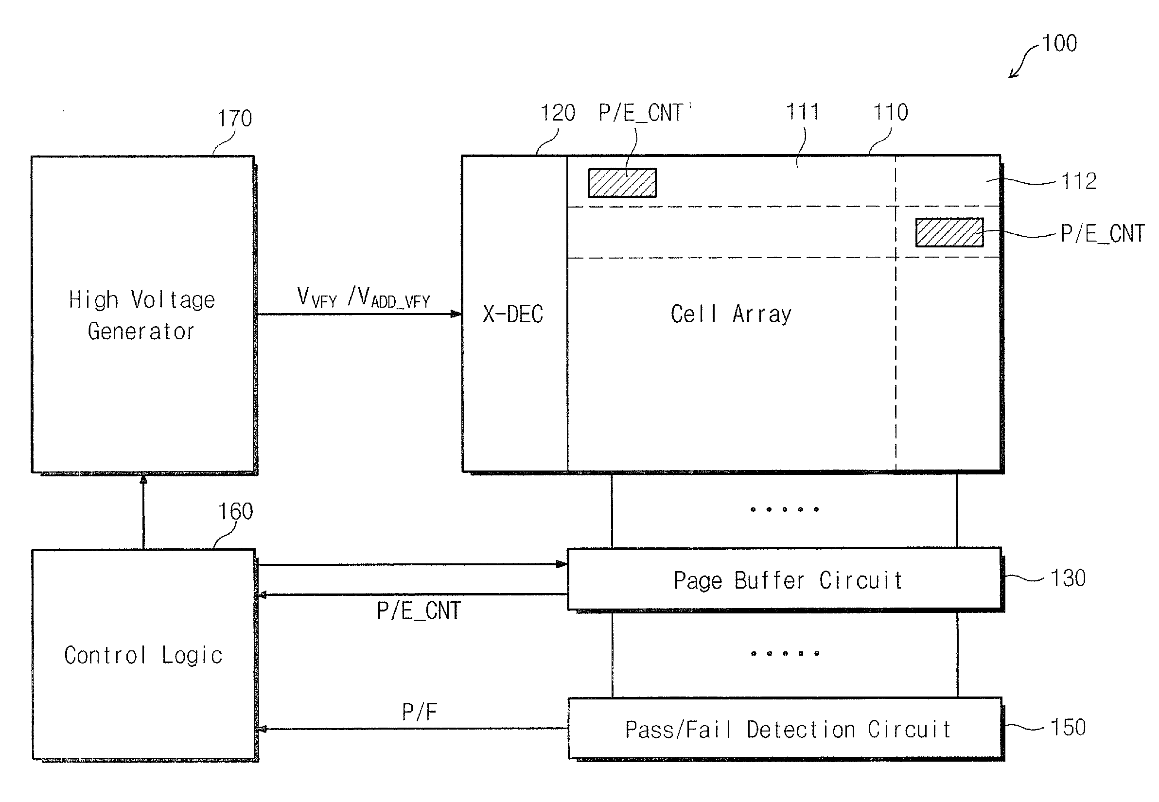
[0024]FIG. 5 is a block diagram of a flash memory device 100 according to an embodiment of the present invention, illustrating a functional structure of a NAND-type flash memory device. Embodiments of the invention may also include NOR-type flash memory devices, for example. Referring to FIG. 5, the flash memory device 100 is illustrated as including a memory cell array 110, an X-decoder 120, a page buffer circuit 130, a pass / fail detection circuit...


PUM


Abstract

Disclosed is a method of verifying a programmed condition of a flash memory device, being comprised of: determining a level of an additional verifying voltage in response to the number of programming / erasing cycles of memory cells; conducting a verifying operation to programmed memory cells with an initial verifying voltage lower than the additional verifying voltage; and selectively conducting an additional verifying operation with the additional verifying voltage to the program-verified memory cells in response to the number of programming / erasing cycles.

Description

REFERENCE TO PRIORITY APPLICATION[0001]This U.S. non-provisional patent application claims priority under 35 U.S.C. § 119 to Korean Patent Application No. 2006-116004, filed Nov. 22, 2006, the contents of which are hereby incorporated herein by reference.FIELD OF THE INVENTION[0002]The present invention relates to nonvolatile memory devices and, more particularly, to flash memory devices and methods of operating flash memory devices.BACKGROUND OF THE INVENTION[0003]Nonvolatile memory devices are capable of retaining data stored in their cells, without loss, even when power is removed. Flash memories are widely used as a type of non-volatile memory device suitable in portable information apparatuses such as mobile phones, personal digital assistants (PDAs), or digital cameras, for example.[0004]FIG. 1 is a cross-sectional diagram of a conventional flash memory cell. Referring to FIG. 1, a flash memory cell 10 has a source 13 and a drain 14 formed of N+ impurities, and a channel regio...

Claims


Application Information

Patent Timeline
Patent Type & Authority Patents(United States)
IPC IPC(8): G11C11/34
CPCG11C16/3454G11C16/344G11C16/10G11C16/34
Inventor PARK, KI-TAEKIM, YONG-SEOKKIM, KI-NAMLEE, YEONG-TAEK
Owner SAMSUNG ELECTRONICS CO LTD
Why Eureka
Try Eureka