Phase change random access memory device and related methods of operation

a random access memory and phase change technology, applied in the direction of information storage, static storage, digital storage, etc., can solve the problems of not being able to simultaneously program the bits into corresponding memory cells, prams may not be able to simultaneously access 16 phase change memory cells, and conventional pram devices are generally not equipped to provide currents of such high magnitudes

Active Publication Date: 2010-04-20
SAMSUNG ELECTRONICS CO LTD
View PDF11 Cites 9 Cited by
  • Summary
  • Abstract
  • Description
  • Claims
  • Application Information

AI Technical Summary

Problems solved by technology

Unfortunately, conventional PRAM devices can receive several bits of input at the same time but are unable to simultaneously program the bits into corresponding memory cells.
For example, a PRAM may receive 16 inputs through a plurality of pins, but the PRAM may not be able to simultaneously access 16 phase change memory cells.
However, conventional PRAM devices are generally not equipped to provide currents with such high magnitudes.
Unfortunately, in PRAM devices using division program operations, the verify read operation tends to significantly increase programming time.
Accordingly, even though the verify read operation tends to improve the reliability of the PRAM devices, it can hurt the overall performance of the PRAM devices.

Method used


Image

  • Phase change random access memory device and related methods of operation
  • Phase change random access memory device and related methods of operation
  • Phase change random access memory device and related methods of operation

Examples


Embodiment Construction

[0031]Exemplary embodiments of the invention are described below with reference to the accompanying drawings. These embodiments are presented as teaching examples while the scope of the invention is defined by the claims that follow.

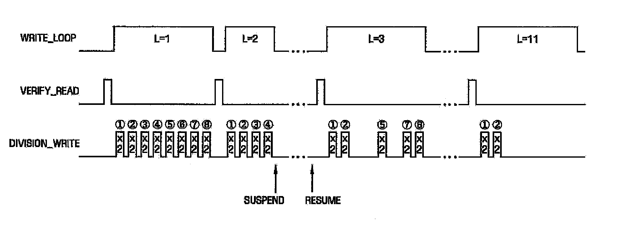
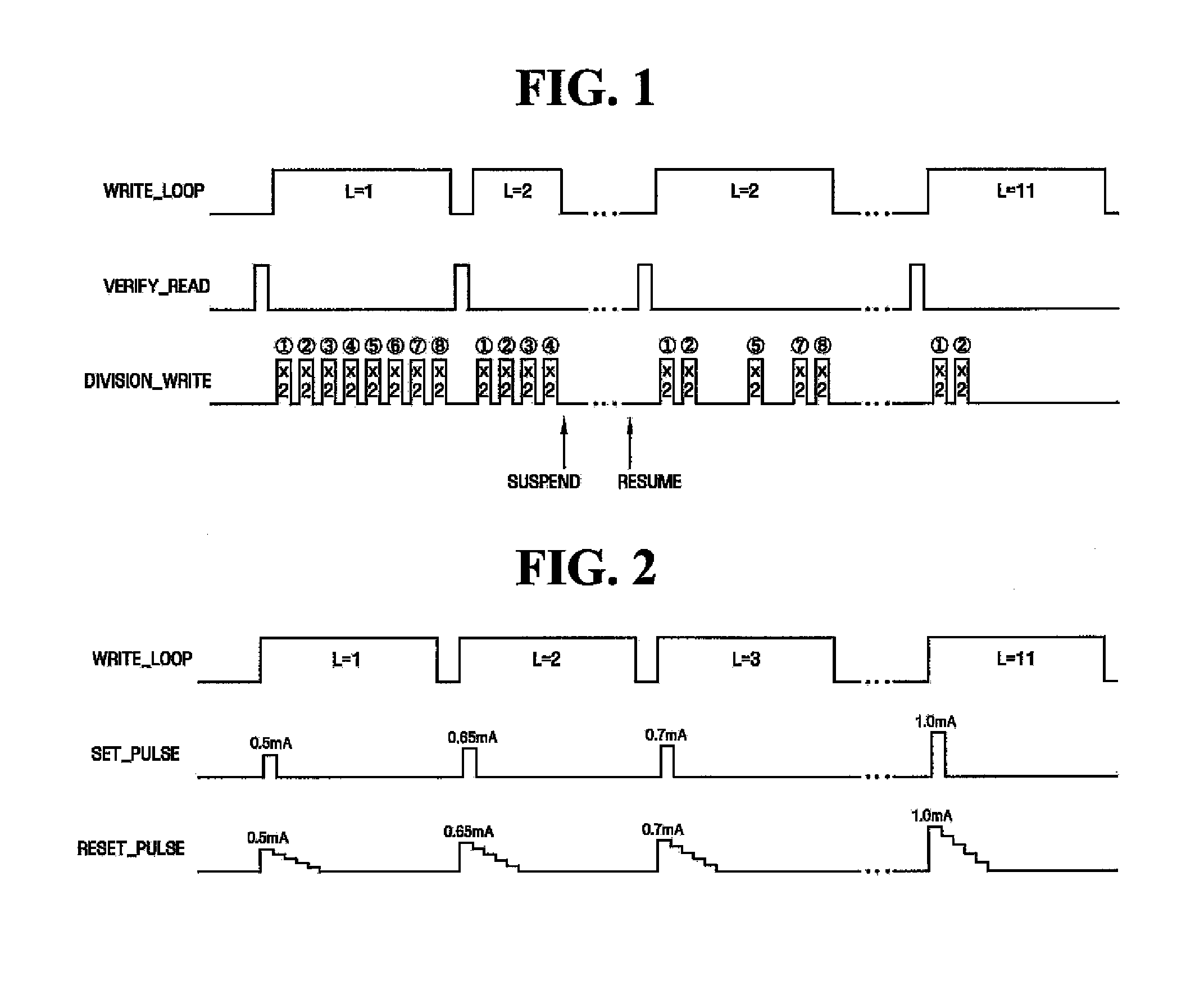
[0032]FIG. 1 is a conceptual timing chart illustrating a method of operating a PRAM device in accordance with an embodiment of the invention.

[0033]Referring to FIG. 1, a program operation is performed in the PRAM device by providing program data to the device and storing a copy of the program data for verify read operations. Next, the program data is programmed into selected phase change memory cells of the PRAM device using a plurality of program loops (L=1 through 11).

[0034]Before the start of each program loop, a verify read operation (VERIFY_READ) is performed to determine whether the selected memory cells have been successfully programmed. In each program loop, a division program operation is performed on selected memory cells that have not been suc...


PUM


Abstract

A method of operating a phase change random access memory (PRAM) device comprises performing a program operation to store data in selected PRAM cells of the device, wherein the program operation comprises a plurality of sequential program loops. The method further comprises suspending the program operation in the middle of the program operation, and after suspending the program operation, resuming the program operation in response to a resume command.

Description

CROSS-REFERENCE TO RELATED APPLICATIONS[0001]This application claims the priority of Korean Patent Application No. 10-2006-0083544, filed on Aug. 31, 2006, the disclosure of which is hereby incorporated by reference in its entirety.BACKGROUND OF THE INVENTION[0002]1. Field of the Invention[0003]Embodiments of the invention relate generally to phase change random access memory (PRAM) devices and related methods of operation. More particularly, embodiments of the invention relate to PRAM devices and related methods for performing program operations.[0004]2. Description of Related Art[0005]Phase change memory devices store data using phase change materials, such as chalcogenide, which are capable of stably transitioning between amorphous and crystalline phases. The amorphous and crystalline phases (or states) exhibit different resistance values used to distinguish different logic states of memory cells in the memory devices. In particular, the amorphous phase exhibits a relatively high...

Claims


Application Information

Patent Timeline
Patent Type & Authority Patents(United States)
IPC IPC(8): G11C11/00
CPCG11C11/5678G11C13/0004G11C13/0069G11C13/0064G11C2013/0092G11C7/1096
Inventor KIM, HYE-JINLEE, KWANG-JINKIM, DU-EUNG
Owner SAMSUNG ELECTRONICS CO LTD
Why Eureka
Try Eureka