CMOS image sensor pixel with selectable binning and conversion gain

a pixel and image sensor technology, applied in the field of image sensors, can solve the problems of inability to select the pixel pixel pixel binning, the disadvantage of reducing the fill factor of the pixel, and the small charge-to-voltage conversion region to hold all the charge that is accumulated in the photodetector, so as to achieve the effect of reducing the resolution readout and high data ra

Active Publication Date: 2010-04-27
OMNIVISION TECH INC
View PDF11 Cites 39 Cited by
  • Summary
  • Abstract
  • Description
  • Claims
  • Application Information

AI Technical Summary

Benefits of technology

[0009]The present invention discloses a CMOS active pixel having the advantages of: (a) single four-transistor operation with global shutter; (b) selectable conversion gain by use of components in adjacent pixels; (c) selectable charge domain binning in both the vertical or horizontal direction; (d) higher data rate for reduced resolution readout; and (e) pixel symmetry since all pixels are identical.

Problems solved by technology

A first disadvantage is that for large pixel sizes, the capacitance of the charge-to-voltage conversion region can be too small to hold all of the charge that is accumulated in the photodetector.
A second disadvantage is lack of in-pixel charge domain binning.
While this solves the charge-to-voltage conversion region capacitance, and can provide a more linear output response, it has the disadvantage of reducing the fill factor of the pixel due to the area in the pixel allocated to the added capacitance Cadd.
The reduced fill factor, adversely affects the charge capacity and dynamic range of the pixel.
A first disadvantage is pixel symmetry.
Each pixel is not identical, and this can lead to systematic differences in photoresponse, causing fixed pattern noise that can degrade image quality.
A second disadvantage is lack of global shutter capability.
Since the charge-to-voltage conversion region is shared by adjacent pixels, it cannot be used as a charge storage region to isolate the signal captured by individual photodetectors.

Method used


Image

  • CMOS image sensor pixel with selectable binning and conversion gain
  • CMOS image sensor pixel with selectable binning and conversion gain
  • CMOS image sensor pixel with selectable binning and conversion gain

Examples


Embodiment Construction

[0024]Before discussing the invention in detail, it is instructive to clearly define CMOS active pixel sensor. CMOS refers to complimentary metal oxide silicon transistors in which complimentary means there are two transistors operating together which are composed of different dopants, one of n-type dopant and one of p-type dopant. The n-type dopant transistor is referred to as NMOS, and the p-type dopant transistor is referred to as PMOS. Active pixel sensors refer to electronic image sensors with active devices, such as transistors, that are associated with each pixel.

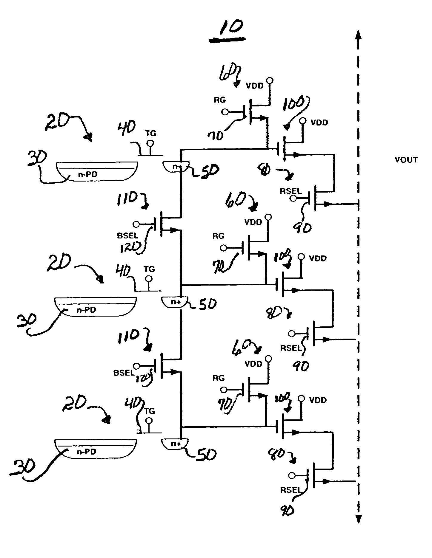
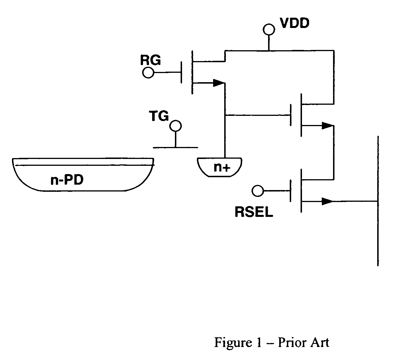
[0025]Now referring to FIG. 4, the CMOS active pixel image sensor 10 of the present invention is shown one embodiment of the present invention that enables charge domain binning in a selectable manner. As seen in FIG. 1, this is in its simplest embodiment a five-transistor pixel. Each pixel 20 includes a photodetector 30, preferably an n-type photodetector for capturing incident light that is converted into charge. A...


PUM


Abstract

An image sensor includes a plurality of pixels, at least two pixels each having a photodetector; a charge-to-voltage conversion region; an input to an amplifier; and a switch for selectively connecting the charge-to-voltage conversion regions.

Description

CROSS-REFERENCE TO RELATED APPLICATIONS[0001]This is a 111A application of Provisional Application Ser. No. 60 / 686,104, filed Jun. 1, 2005.FIELD OF THE INVENTION[0002]The invention relates generally to the field of image sensors, and more particularly, to image sensors having pixels that can selectively combine charge-to-voltage conversion regions.BACKGROUND OF THE INVENTION[0003]Prior art CMOS Active Pixel Sensor pixel architectures are shown in FIGS. 1, 2 and 3. Referring to FIG. 1, this four-transistor pixel has a photodetector n-PD and a charge-to-voltage conversion region n+ in each pixel. This architecture provides the some advantages. The first advantage is global shutter operation by using the charge-to-voltage conversion region n+ as a storage region. The second advantage is pixel symmetry. Each pixel is identical which provides identical photoresponse for each pixel. This pixel architecture also has disadvantages. A first disadvantage is that for large pixel sizes, the cap...

Claims


Application Information

Patent Timeline
Patent Type & Authority Patents(United States)
IPC IPC(8): H04N3/14H01L27/00H01L31/062H04N5/345H04N5/347H04N5/365H04N5/374H04N9/07
CPCH01L27/14643H04N3/1562H04N5/3745H04N5/347H04N5/3559H01L27/14641H04N25/46H04N25/59H04N25/77H04N25/60
Inventor GUIDASH, R. MICHAEL
Owner OMNIVISION TECH INC
Why Eureka
Try Eureka