Method and arrangement for producing a smart card

a smart card and arrangement technology, applied in the direction of antennas, antenna adaptation in movable bodies, electromagnets, etc., can solve the problems of only testing the wire connectors or antenna coils of a smart card produced according to a conventional method, and is much more expensive than substrates and antenna coils, so as to achieve less mechanical stress

Active Publication Date: 2010-05-04
RUHLAMAT
View PDF19 Cites 6 Cited by
  • Summary
  • Abstract
  • Description
  • Claims
  • Application Information

AI Technical Summary

Benefits of technology

[0011]In an embodiment, the antenna coil may be arranged around the mounting location. In this case the wire connector exhibits an intersection. In another embodiment the antenna coil is arranged so that a part of it traverses the mounting location. The chip module is inserted on top of this part in this case. The advantage of this embodiment is that an intersection of the wire connector may be avoided, thus saving headroom. Furthermore the wire connector does not necessarily have to be insulated in this embodiment. However, slightly more headroom is demanded in the area of the chip module because of the wire connector running below.
[0013]In another embodiment of the invention the shape of the second section is achieved by guiding it around an auxiliary tool to determine the shape of the contacting loop by means of the wire guiding unit. The auxiliary tool, e.g. which can be in the shape of a pin, should be placeable in a position between the surface and the second section and removeable from this position. Thus the contacting loop may be given, for example, an Omega-shape, thereby resulting in a particularly good stress relief.
[0018]In another embodiment, at least one additional film may be attached to at least one of the two surfaces of the substrate, particularly another thermoplastic film. In particular, if the mounting location is designed as an aperture, an additional film may be attached below the substrate in order to support the chip module. Another additional film may be placed on top of the chip module after the wiring and contacting, also in such a case when the mounting location is not a recess. The additional film to be placed on top of the chip module may exhibit a recess for encasing the chip module. It may as well exhibit a softening temperature which is lower than a softening temperature of the substrate. The substrate and the additional film may be aligned and fixed together in at least two areas by, for example, heat, pressure, or energy provided by the ultrasonic sonotrode in order to ease the handling of the smart card without affecting the contacts.

Problems solved by technology

By contrast, the wire connectors or antenna coils of a smart card produced according to a conventional method can only be tested when the chip module is already inserted and contacted.
Chip modules for application in passports according to ICAO 9303 contain particularly large integrated circuits with an EEPROM capacity of at least 64 kBit and are much more expensive than the substrates and antenna coils.

Method used


Image

  • Method and arrangement for producing a smart card
  • Method and arrangement for producing a smart card
  • Method and arrangement for producing a smart card

Examples


Embodiment Construction

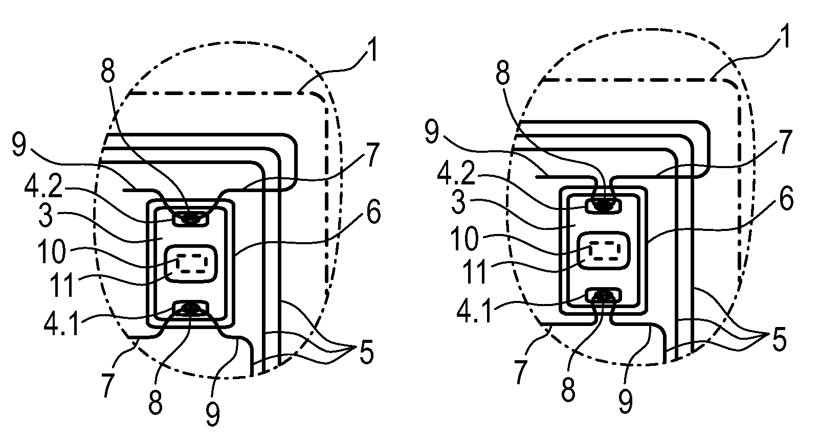
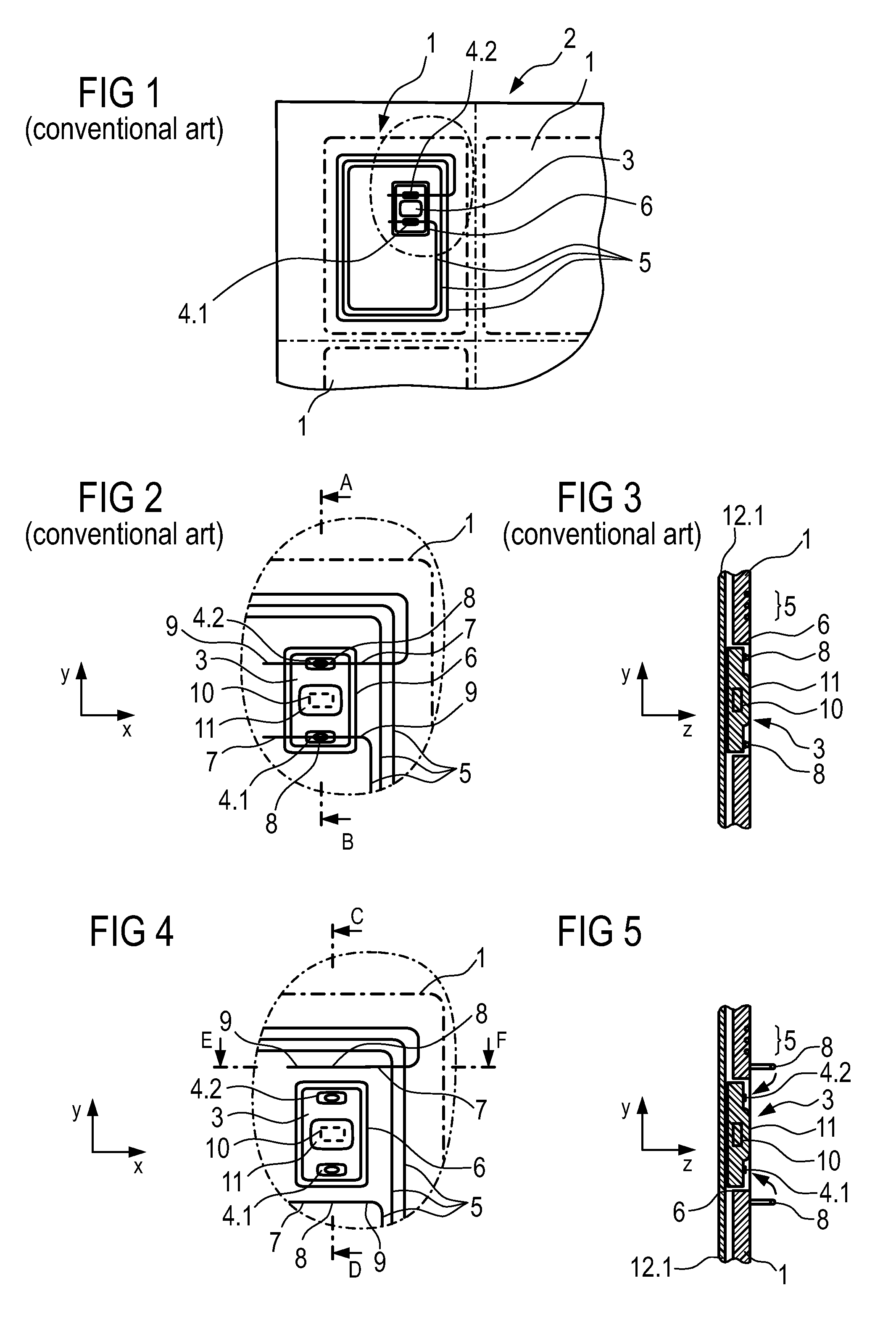
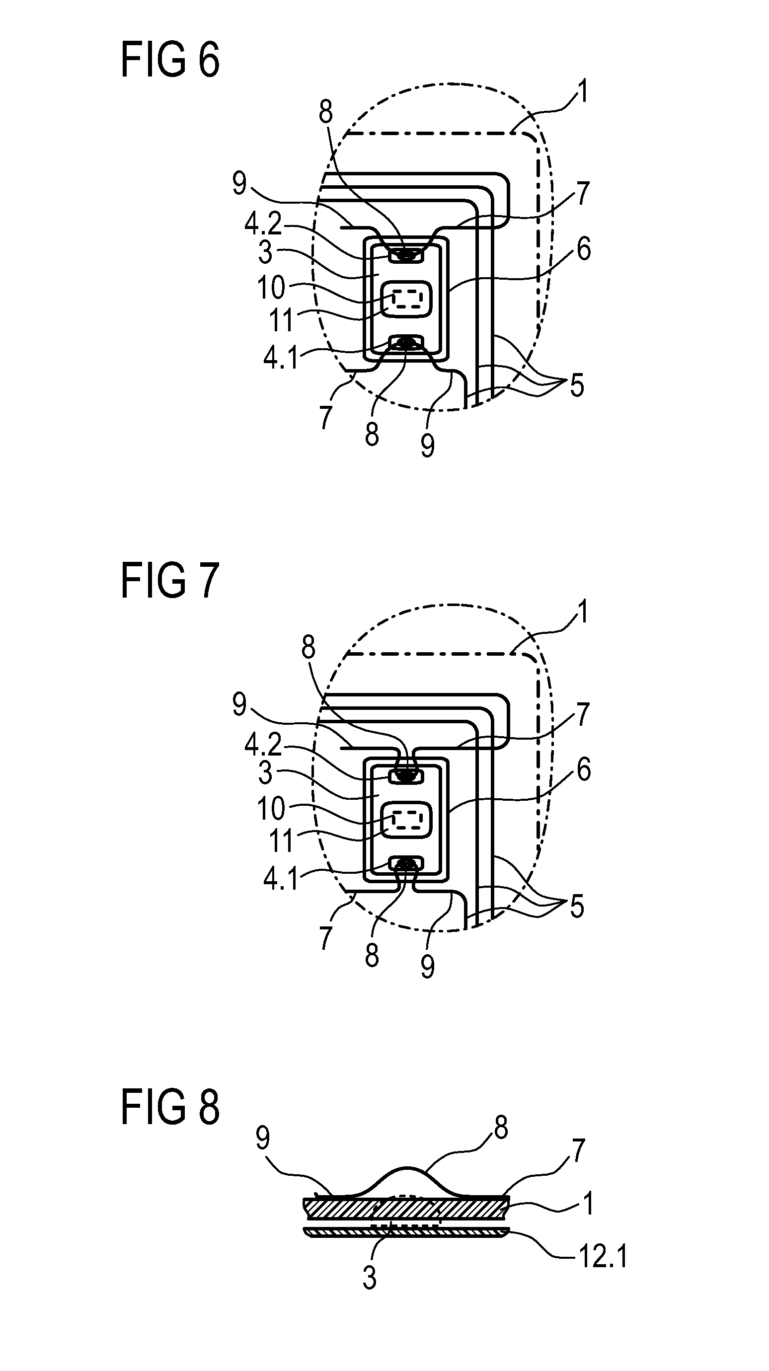
[0033]FIG. 1 is a top view of a substrate 1 of a smart card, which can be one of a multitude of segments of a multi-image-board 2. The smart card 1 comprises a chip module 3 with two contacting areas 4.1, 4.2 and a wire connector 5 in the shape of an antenna coil arranged around the chip module 3. The wire connector 5 is laid, attached and contacted. The chip module 3 is attached on the substrate 1 in a mounting location 6, which may be designed as a recess in the substrate 1. For producing the smart card, the substrate 1, which can also be in single-image-format, is placed on a bench. The chip module 3 is arranged in the mounting location 6 with the contacting areas 4.1, 4.2 up. If the mounting location 6 is a recess in the form of an aperture, the chip module 3 may be fixed by a vacuum from below or by attaching it to an additional film (not shown) that is arranged below the substrate 1.

[0034]The wire connector 5 is attached to a surface of the substrate 1 or at least partially em...


PUM

PropertyMeasurementUnit
thicknessaaaaaaaaaa
contacting areaaaaaaaaaaa
areasaaaaaaaaaa

Abstract

A method is provided for producing a smart card comprising a chip module with at least one contacting area, the chip module arrangeable in a mounting location of a substrate, wherein one contacting loop is formed from a wire connector fed by a wire guiding unit for at least one of the contacting areas, respectively by attaching a first section of the wire conductor to a surface of the substrate outside the mounting location, wherein a second section of the wire conductor proximate to the first section is guided to form the contacting loop along with and protruding from the surface, wherein a subsequent third section of the wire conductor is attached to the surface outside the mounting location, wherein the chip module is inserted into the mounting location and wherein the second section is bent over and electrically contacted to the contacting area.

Description

BACKGROUND OF THE INVENTION[0001]1. Field of the Invention[0002]The invention refers to a method and an arrangement for producing a smart card.[0003]2. Description of the Background Art[0004]Documents, such as passports, identity documents and ID-cards, particularly in the formats ID-1, ID-2 and ID-3 are often equipped with RFID (Radio Frequency Identification Device) systems according to the ICAO 9303 specification. Normally an RFID transponder with an antenna coil is applied for this purpose. The antenna coil can be produced by etching a copper or aluminium film, by silkscreen printing or by inkjet printing with electrically conductive pastes. Alternatively, thin enamel-insulated copper wires with 30 μm to 150 μm thickness are run on an inner layer, a chip module is inserted on the inner layer or a recess thereof and the wire ends are contacted to the chip module.[0005]The European Patent EP 0 880 754 B1, which corresponds to U.S. Pat. No. 6,233,818, discloses a process for the co...

Claims


Application Information

Patent Timeline
Patent Type & Authority Patents(United States)
IPC IPC(8): H01Q13/00H01Q1/28
CPCG06K19/07749G06K19/0775H01L23/49855H01L24/85Y10T29/49128Y10T29/4913Y10T29/49018Y10T29/49073Y10T29/49002Y10T29/49016H01L24/45H01L2224/45147H01L2224/78744H01L2224/85H01L2224/85205H01L2224/85214H01L2924/14H01L2924/00015H01L2924/00014H01L2924/00
Inventor KOCH, MATTHIASGEBHARDT, BERND
Owner RUHLAMAT
Why Eureka
Try Eureka