Charge pump circuit and cell thereof

a charge pump and circuit technology, applied in the field of charge pump circuit and cell, can solve the problems of low supply voltage, poor charge pump circuit performance, and low b>10/b> performance, and achieve the effects of saving power consumption, high driving capability, and fast start-up tim

Active Publication Date: 2010-05-11
ELITE SEMICON MEMORY TECH INC
View PDF6 Cites 17 Cited by
  • Summary
  • Abstract
  • Description
  • Claims
  • Application Information

AI Technical Summary

Benefits of technology

[0021]Accordingly, compared to the conventional charge pump circuit, the charge pump circuit provided by the embodiment of the invention has fast start-up time and high driving capability. Thus the charge pump circuit provided by the embodiment can save power consumption and be suitable for high speed circuit.

Problems solved by technology

However, the supply voltage is usually low, and thus a charge pump circuit is needed in the semiconductor memories.
The capacitors C(1)˜C(N) and Cout have the size limitations in the practical implementation, and thus the performance of the charge pump circuit 10 may be poor.
However, the start-up time of the charge pump circuit 30 is not improved, and thus it is not suitable for the high speed operation system.
However, the critical timing control increases the complexity of the charge pump circuit 50, and thus the charge pump circuit 50 may not operate at high speed.
Although the charge pump circuit 70 has reduced the body effect and improved the efficiency, the driving capability and the start-up time have not been improved.

Method used


Image

  • Charge pump circuit and cell thereof
  • Charge pump circuit and cell thereof
  • Charge pump circuit and cell thereof

Examples


Embodiment Construction

[0042]Reference will now be made in detail to the present preferred embodiment of the invention, examples of which are illustrated in the accompanying drawings. Wherever possible, the same reference numbers are used in the drawings and the description to refer to the same or like parts.

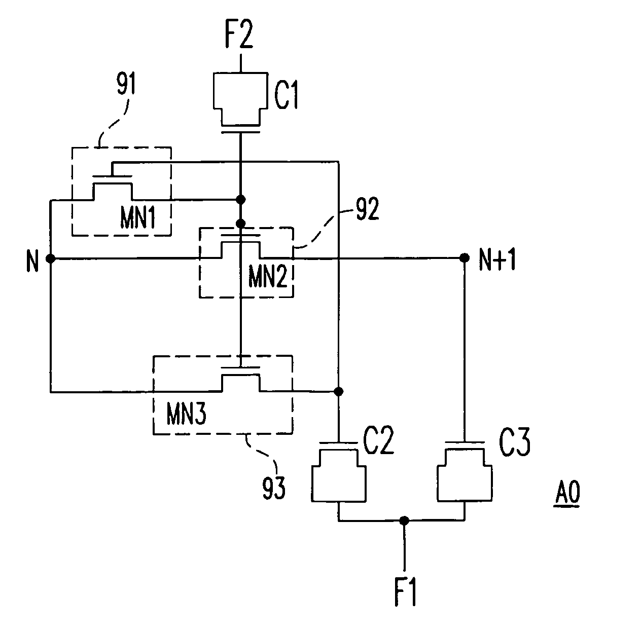
[0043]Referring to FIG. 9, FIG. 9 is a circuit diagram of a charge pump cell 90 according to one embodiment of the present invention. The charge pump cell 90 with an input and output nodes N, N+1 includes a plurality of equalization unit 91, 92 and 93, and a plurality of capacitors C1, C2 and C3. Each of the equalization units 91, 92 and 93 is used for equalizing the charges of its input and output.

[0044]Wherein the input node N is coupled to the inputs of the equalization units 91, 92 and 93. The output node N+1 is also coupled to the equalization unit 92. One end of the capacitor C2 is coupled to the control end of the equalization unit 91 for enabling or disabling the equalization unit 91, and also...


PUM


Abstract

A charge pump cell with an input and output nodes includes a first, second, and third equalization units, and a first, second, and third capacitors. The input node is coupled to the inputs of the first, second and third equalization units, and the output node is coupled to the second equalization unit. One end of the second capacitor is coupled to the control end of the first equalization unit for enabling or disabling the first equalization unit, and also coupled to the output of the third equalization unit. One end of the third capacitor is coupled to the output of the second equalization unit. One end of the first capacitor is coupled to the control ends of the second and third equalization units, and also coupled to the output of the first equalization unit.

Description

CROSS-REFERENCE TO RELATED APPLICATION[0001]This application claims the priority benefit of U.S. provisional application Ser. No. 60 / 989,985, filed on Nov. 26, 2007. The entirety of the above-mentioned patent application is hereby incorporated by reference herein and made a part of this specification.BACKGROUND OF THE INVENTION[0002]1. Field of Invention[0003]The present invention generally relates to the charge pump circuit and cell thereof, and more particularly to the charge pump circuit and cell thereof with faster start-up time.[0004]2. Description of Prior Art[0005]The semiconductor memories need a high voltage for writing data. However, the supply voltage is usually low, and thus a charge pump circuit is needed in the semiconductor memories.[0006]Referring to FIGS. 1 and 2, FIG. 1 is a circuit diagram of a conventional charge pump circuit 10, and FIG. 2 is a waveform diagram of the clock signals in the charge pump circuit 10. The charge pump circuit 10 is a Dickson charge pum...

Claims


Application Information

Patent Timeline
Patent Type & Authority Patents(United States)
IPC IPC(8): G05F1/10
CPCH02M3/073
Inventor CHANG, CHIEN-YIHUA, CHUNG-HSIEN
Owner ELITE SEMICON MEMORY TECH INC
Why Eureka
Try Eureka