Sub-mount for mounting optical component, manufacturing method thereof, and light transmission and reception module

a technology for optical components and manufacturing methods, applied in the direction of optical elements, instruments, optical waveguide light guides, etc., can solve the problems of large devices, large mounting costs, and need for expensive devices such as rie, and achieve the effect of easy production of high precision

Active Publication Date: 2010-06-08
FUJIFILM BUSINESS INNOVATION CORP
View PDF24 Cites 10 Cited by
  • Summary
  • Abstract
  • Description
  • Claims
  • Application Information

AI Technical Summary

Benefits of technology

[0014]The sub-mount of the invention has the tapered side wall of the recess for mounting, therefore, the optical component is embedded and mounted in the recess easily and reliably. Thus, the sub-mount of the invention excels in mass production with a low cost.
[0017]In the light transmission and reception module of the invention, the side wall of the recess for mounting to embed and mount the optical component is tapered, and thus it is allowed that the optical element serving as the optical component and the optical waveguide film are easily and reliably mounted to the sub-mount at high precision resulting in the module is excels in mass production at a low cost.
[0019]According to the manufacturing method of the sub-mount for mounting an optical component, since the shape including the recess for mounting of the sub-mount is accurately copied to the mold for duplication, the sub-mount maintaining the shape at high precision can be produced easily.

Problems solved by technology

However, the methods proposed so far requires a mirror to be embedded to form a 90° return mirror, and requires positioning at high precision when laminating the waveguide and the light transmission and reception element, and thus the cost required for mounting becomes large.
In Japanese Patent Application Laid-Open No. 5-114800 (1993), a method of causing vibration using ultrasonic to facilitate alignment is contrived when elements are embedded into a recess of sub-mount, but has a disadvantage in that a device becomes large.
An expensive device such as RIE is necessary to manufacture a sub-mount with precise shape.
Further, a mounting device of high precision is necessary in order to accurately mount the elements into the recess of the high-precision processed sub-mount, and thus the mounting cost increases.

Method used


Image

  • Sub-mount for mounting optical component, manufacturing method thereof, and light transmission and reception module
  • Sub-mount for mounting optical component, manufacturing method thereof, and light transmission and reception module
  • Sub-mount for mounting optical component, manufacturing method thereof, and light transmission and reception module

Examples


example

[0144]The invention is more specifically described below by referring to an example, but the invention is not limited to the example alone.

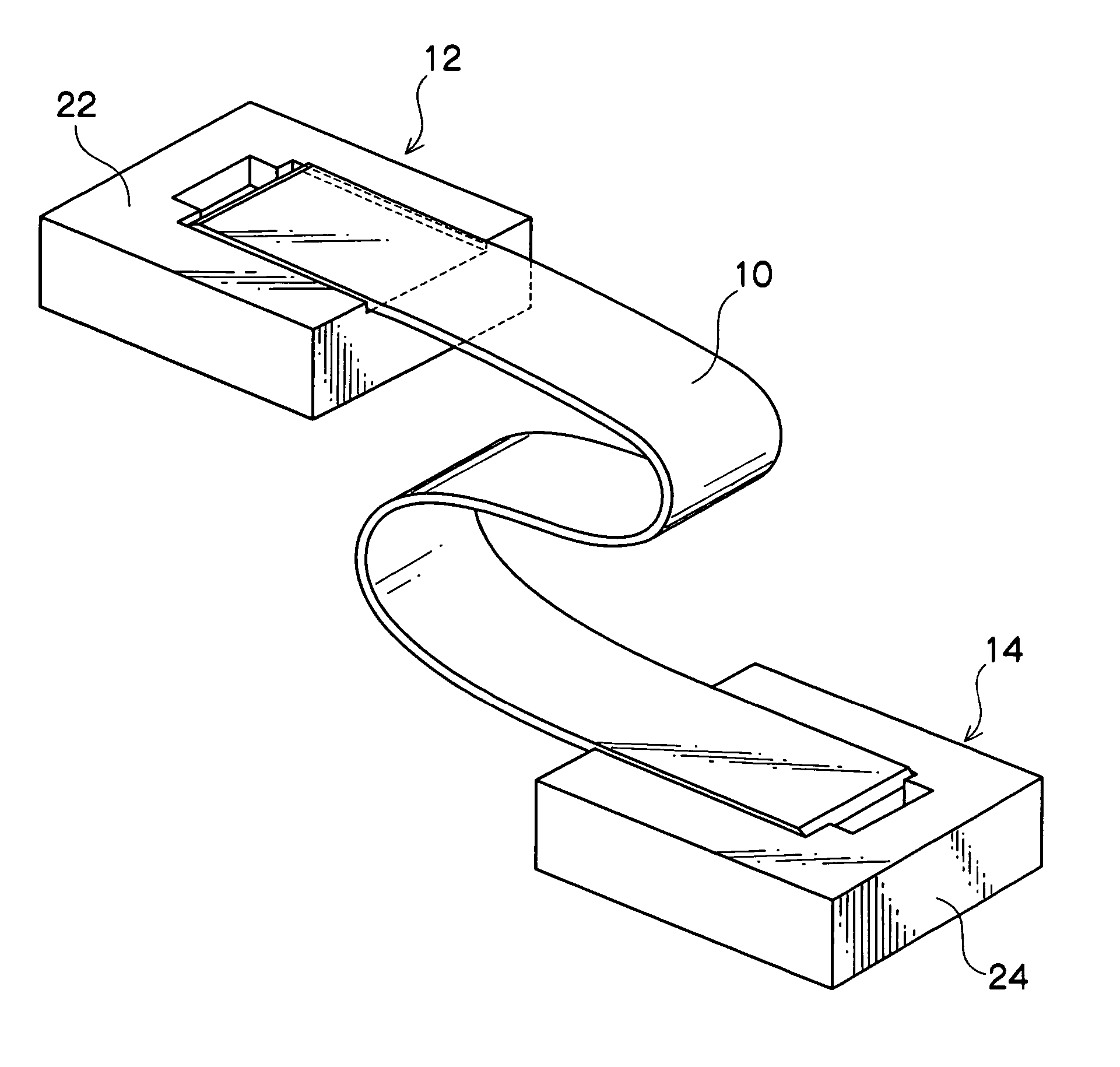
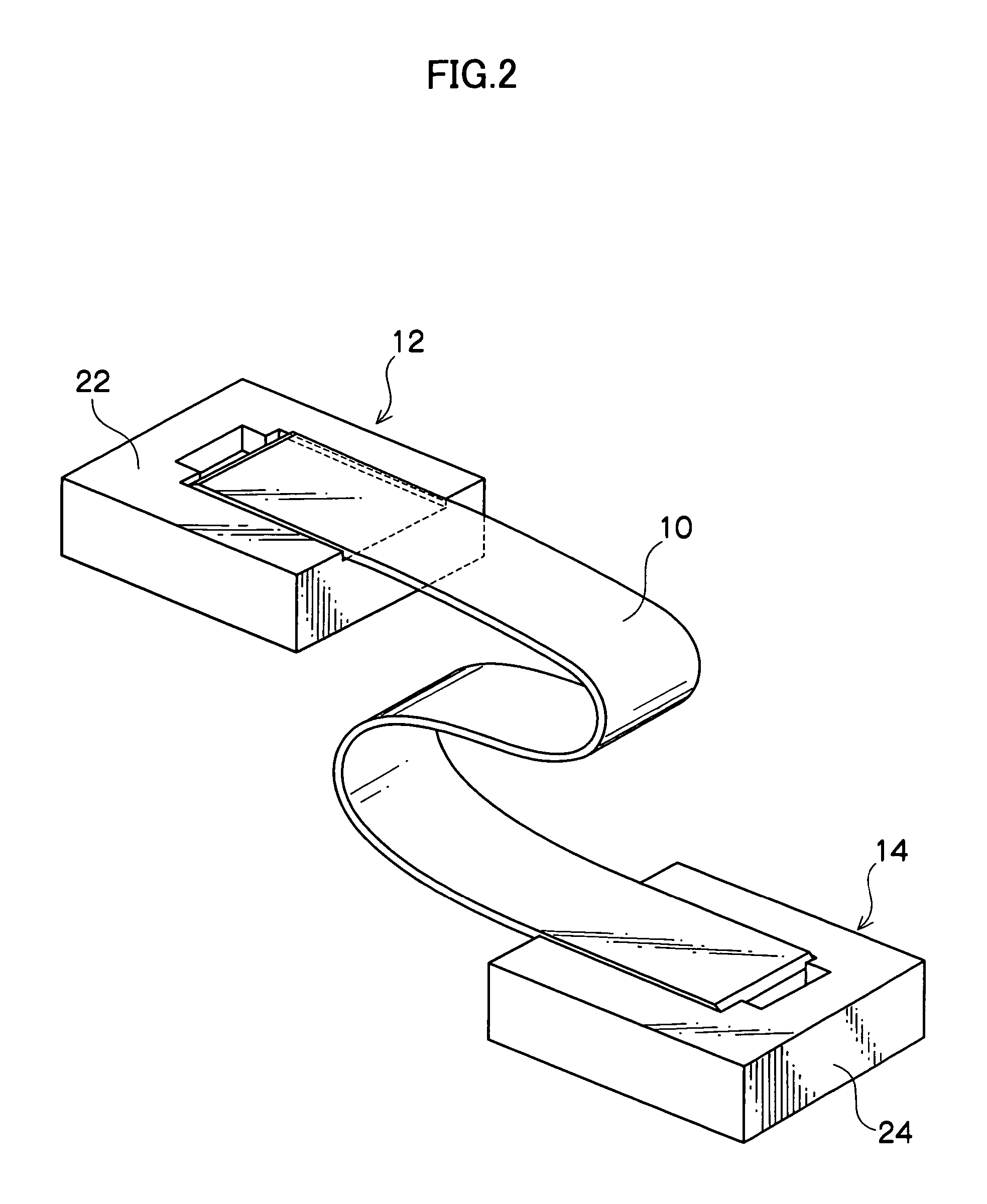
[0145]An example of producing a mold from a master mold (a master plate) using silicone resin, duplicating a sub-mount using epoxy resin of UV curing type, and producing a light transmission and reception module is given. A recess having a tapered side wall is referred to as “tapered recess”.

(Production of Macromolecule Optical Waveguide Film)

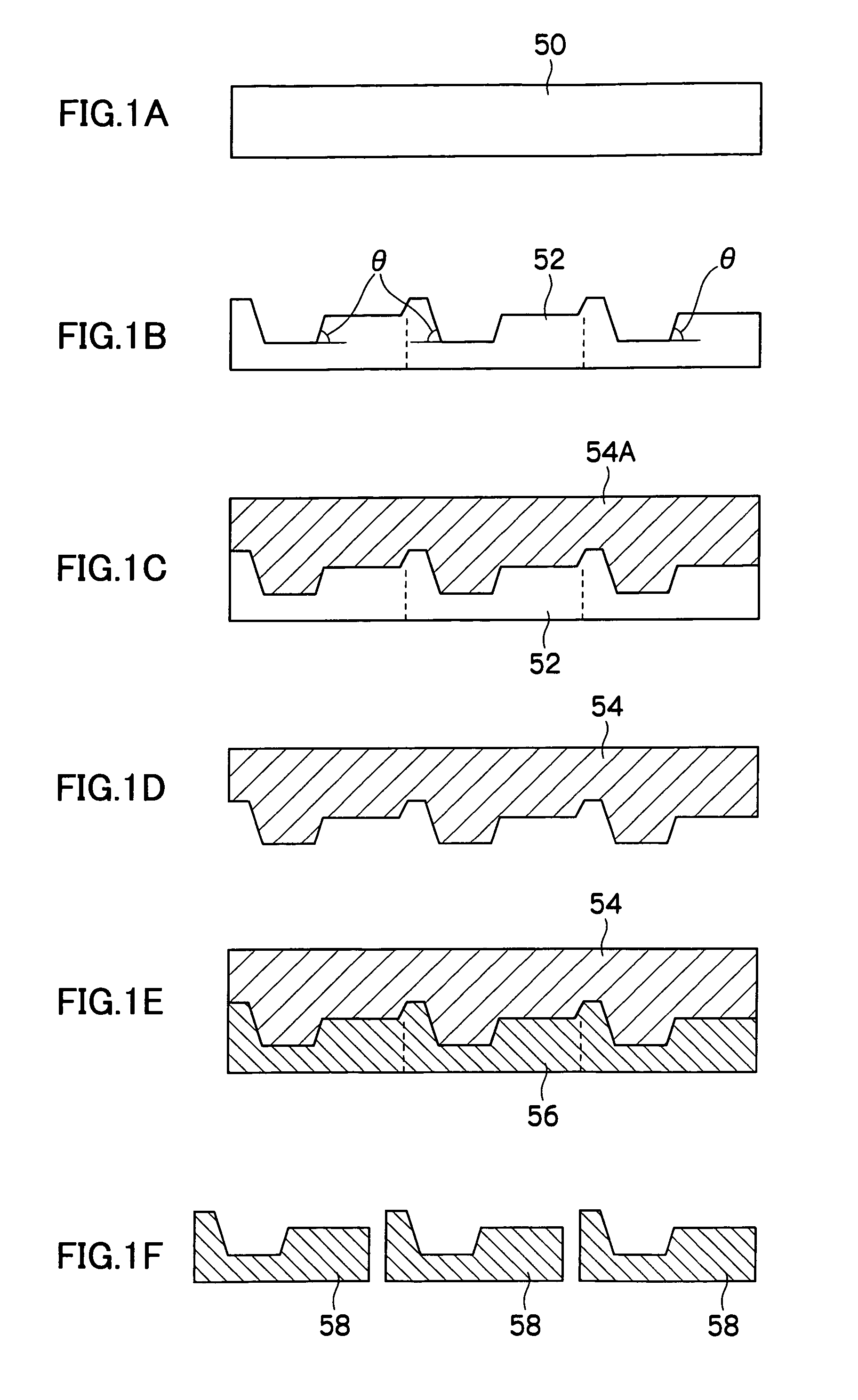
[0146]After an Si substrate is coated with a thick film resist (trade name: SU-8, manufactured by Microchemical) according to a spin coat method, it is prebaked at 80 deg. C., is exposed through a photomask and is developed so that four projections respectively having a quadrate section (width: 50 μm, height: 50 μm, length: 80 mm) are formed. Each gap between the projections is set to 250 μm. The Si substrate coated with the thick film resist is post-baked at 120 deg. C., so that a master plate for manufactu...


PUM


Abstract

A sub-mount for mounting optical components includes a recess for mounting whose side wall is tapered. A light transmission and reception module includes the sub-mount for mounting optical component. The sub-mount is manufactured by forming a master mold of the sub-mount formed with projections and recesses including the recess for mounting of the sub-mount, applying liquid silicone rubber to the mater mold, curing the liquid silicone rubber to produce a mold for duplication, filling the curable material into the mold for duplication, curing the curable material, and separating the cured curable material from the mold for duplication.

Description

CROSS-REFERENCE TO RELATED APPLICATION[0001]This application claims priority under 35 USC 119 from Japanese patent document, No. 2005-214936, the disclosure of which is incorporated by reference herein.FIELD OF THE INVENTION[0002]The present invention relates to a sub-mount for mounting optical component, light transmission and reception modules, and manufacturing method of the sub-mount for mounting optical component, more specifically, relates to a sub-mount mounted inside a package of an optical device, a light transmission and reception module using the sub-mount, and a manufacturing method of the sub-mount.DESCRIPTION OF THE RELATED ART[0003]Recently, in IC technique or LSI technique, optical wiring between equipments, between boards in the equipments, or in a chip is given attention instead of the electrical wiring at high density to enhance the operating speed or integration degree.[0004]In Japanese Patent Application Laid-Open No. 2000-39530, for example, an optical element ...

Claims


Application Information

Patent Timeline
Patent Type & Authority Patents(United States)
IPC IPC(8): G02B6/36
CPCG02B6/4214G02B6/4246G02B6/43H01L24/73H01L2924/01046H01L2924/01079H01L2224/45144H01L2224/48227H01L2224/48472H01L2224/49171H01L2924/01019H01L2224/48091H01L2924/00014H01L2924/00H01L2924/12043H01L2924/14H01L2924/15153
Inventor OHTSU, SHIGEMISUZUKI, TOSHIHIKOSHIMIZU, KEISHIYATSUDA, KAZUTOSHIFUJII, AKIRAAKUTSU, EIICHI
Owner FUJIFILM BUSINESS INNOVATION CORP
Why Eureka
Try Eureka