Semiconductor integrated circuit device

a technology of integrated circuits and semiconductors, applied in semiconductor devices, instruments, computing, etc., can solve the problems of affecting the design of integrated circuits, affecting the performance of circuits, and reducing yield, so as to achieve suppressed variations in transistor characteristics due to the well proximity

Active Publication Date: 2010-06-15
SOCIONEXT INC
View PDF5 Cites 112 Cited by
  • Summary
  • Abstract
  • Description
  • Claims
  • Application Information

AI Technical Summary

Benefits of technology

[0016]An object of the present invention is to provide a semiconductor integrated circuit device in which variations in transistor characteristics due to the well proximity effect can be suppressed.
[0018]In the first embodiment of the present invention, in at least one of the standard cell rows, the distance from a PMOS transistor located at least one end thereof to an end closer to the PMOS transistor in the horizontal direction of the N well is greater than or equal to the shared-N well width which is a width in the vertical direction of the N well shared by the second and third standard cell rows. Therefore, the well proximity effect at an end portion of a standard cell row can be suppressed, so that a difference in characteristics between a transistor located at the end of the standard cell row and transistors located elsewhere can be suppressed.
[0020]In the second embodiment of the present invention, the width in the vertical direction of the N well in the first standard cell row is greater than or equal to the shared-N well width which is a width in the vertical direction of the N well shared by the second and third standard cell rows. Therefore, the well proximity effect in the first standard cell row can be suppressed to the same extent to which the well proximity effect in the second and third standard cell rows is suppressed. A difference in characteristics between transistors in the first standard cell row and transistors in the second and third standard cell rows can be suppressed.
[0022]In the third embodiment of the present invention, in at least one of the standard cell rows, the distance from an NMOS transistor located at least one end thereof to an end closer to the NMOS transistor in the horizontal direction of the P well is greater than or equal to the shared-P well width which is a width in the vertical direction of the P well shared by the second and third standard cell rows. Therefore, the well proximity effect at an end portion of a standard cell row can be suppressed, so that a difference in characteristics between a transistor located at the end of the standard cell row and transistors located elsewhere can be suppressed.
[0024]In the fourth embodiment of the present invention, the width in the vertical direction of the P well in the first standard cell row is greater than or equal to the shared-P well width which is a width in the vertical direction of the P well shared by the second and third standard cell rows. Therefore, the well proximity effect in the first standard cell row can be suppressed to the same extent to which the well proximity effect in the second and third standard cell rows is suppressed. A difference in characteristics between transistors in the first standard cell row and transistors in the second and third standard cell rows can be suppressed.
[0025]As described above, according to the present invention, variations in transistor characteristics due to the well proximity effect can be suppressed.

Problems solved by technology

Therefore, there is a mismatch between the design and the product in terms of circuit operation timing or the like, resulting in a defective product.
In addition, a decrease in yield, a decrease in circuit performance due to addition of a design margin for securing a difference in characteristics, and an increase in block area lead to a reduction in competitiveness.
The above-described problem has become significant with the development of even smaller microstructures.

Method used


Image

  • Semiconductor integrated circuit device
  • Semiconductor integrated circuit device
  • Semiconductor integrated circuit device

Examples


first embodiment

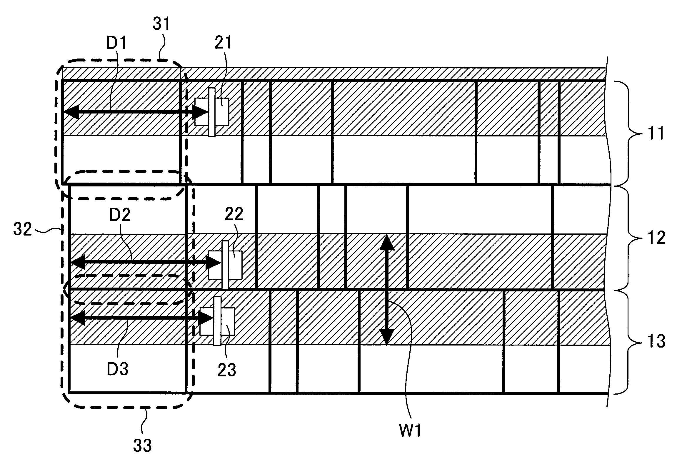
[0078]FIG. 1 is a diagram showing a portion of a layout of a semiconductor integrated circuit device according to a first embodiment of the present invention. In FIGS. 1, 11, 12 and 13 indicate standard cell rows in which standard cells 10 (illustrated with rectangles) are arranged in the horizontal direction. The standard cell rows 11, 12, 13, . . . are arranged in the vertical direction to form a circuit block. The standard cell row 11 is the uppermost row. Each of the standard cell rows 11, 12 and 13 includes an N well and a P region which extend in the horizontal direction and are adjacent to each other in the vertical direction. Each standard cell 10 has a PMOS transistor formed in the N well and an NMOS transistor formed in the P region. Note that transistors other than PMOS transistors 21, 22 and 23 are not shown.

[0079]The semiconductor integrated circuit device of FIG. 1 has an N-well structure in which PMOS transistors are formed on an N well and NMOS transistors are formed...

second embodiment

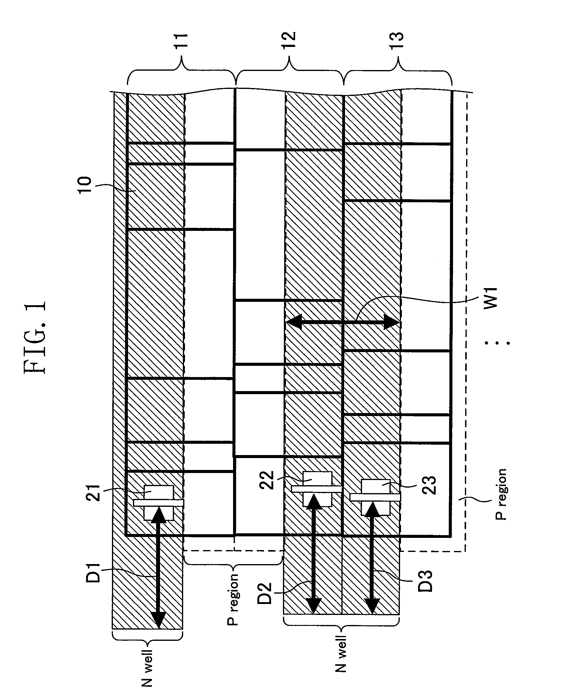
[0096]FIG. 9 is a diagram showing a portion of a layout of a semiconductor integrated circuit device according to a second embodiment of the present invention. The semiconductor integrated circuit device of FIG. 9 has substantially the same configuration as that of FIG. 1. The same parts are indicated by the same symbols. W2 indicates a width in the vertical direction of an N well in a first standard cell row 11.

[0097]In the semiconductor integrated circuit device of FIG. 9, the width W2 in the vertical direction of the N well in the first standard cell row 11 is broadened as compared to the conventional layout of FIG. 26. The width W2 is also greater than or equal to a width (shared-N well width) W1 in the vertical direction of an N well shared by second and third standard cell rows 12 and 13. Thereby, a distance D4 from a PMOS transistor (e.g., a PMOS transistor 21) to a farther end in the vertical direction of the N well in the first standard cell row 11 is greater than or equal ...

third embodiment

[0112]A third embodiment of the present invention is a combination of the first and second embodiments. FIG. 16 is a diagram showing a portion of a layout of a semiconductor integrated circuit device according to the third embodiment of the present invention. The semiconductor integrated circuit device of FIG. 16 has substantially the same configuration as that of FIGS. 1 and 9 and the same parts are indicated by the same symbols.

[0113]In the semiconductor integrated circuit device of FIG. 16, distances D1, D2 and D3 from PMOS transistors 21, 22 and 23 to ends of N wells are broadened to be greater than or equal to a width W1 in the vertical direction of an N well shared by second and third standard cell rows 12 and 13, as in the semiconductor integrated circuit device of FIG. 1. Also, a width W2 in the vertical direction of an N well in a first standard cell row 11 is broadened to be greater than or equal to the width W1 in the vertical direction of the N well shared by the second ...


PUM


Abstract

A semiconductor integrated circuit device capable of suppressing variations in transistor characteristics due to the well proximity effect is provided. Standard cell rows are arranged in a vertical direction, each standard cell row including standard cells arranged in a horizontal direction. In the standard cell rows, positions of the N well and the P region in the vertical direction are switched every other row. Adjacent standard cell rows share the P region or the N well. A distance from a PMOS transistor located at an end of a standard cell row to an end of an N well is greater than or equal to a width of an N well shared by standard cell rows.

Description

CROSS REFERENCE TO RELATED APPLICATIONS[0001]This Non-provisional application claims priority under 35 U.S.C. §119(a) on Patent Application No. 2007-099422 filed in Japan on Apr. 5, 2007 and Patent Application No. 2007-233650 filed in Japan on Sep. 10, 2007, the entire contents of which are hereby incorporated by reference.BACKGROUND OF THE INVENTION[0002]1. Field of the Invention[0003]The present invention relates to a technique for designing the layout of a semiconductor integrated circuit and, more particularly, to a semiconductor integrated circuit device designed by arranging standard cells.[0004]2. Description of the Related Art[0005]Conventionally, the layout of a semiconductor integrated circuit is designed by arranging circuit components called standard cells. For example, standard cells are arranged in a horizontal direction to form a standard cell row, and a plurality of standard cell rows are arranged in a vertical direction to form a circuit block. Each standard cell ha...

Claims


Application Information

Patent Timeline
Patent Type & Authority Patents(United States)
IPC IPC(8): H01L29/72
CPCH01L27/11807H01L27/0207
Inventor KONDO, HIDEAKIMORIWAKI, TOSHIYUKITAMARU, MASAKIANDOH, TAKASHI
Owner SOCIONEXT INC
Why Eureka
Try Eureka