IQ Optical Modulator

a technology of optical modulator and modulator, applied in the field can solve the problems of optical loss, high-frequency characteristics degradation, operation stability problems, etc., and achieve the effect of improving the high-frequency characteristics of iq optical modulator and suppressing the temperature fluctuation of the difference in characteristics between iq channels

Pending Publication Date: 2022-10-13
NIPPON TELEGRAPH & TELEPHONE CORP
View PDF0 Cites 0 Cited by
  • Summary
  • Abstract
  • Description
  • Claims
  • Application Information

AI Technical Summary

Benefits of technology

[0044]With such a configuration, the optical waveguide structure is a symmetrical structure between the IQ channels, and therefore, a difference in characteristics between IQ channels due to temperature fluctuations can be suppressed. Since an RF feeder line length can be reduced, the high-frequency characteristics of the IQ optical modulator improves.

Problems solved by technology

In FIG. 1, since the waveguide structure is symmetric between the IQ channels, the characteristic error between the channels is small with respect to temperature fluctuation and temperature distribution within the chip, but there is a concern for degradation of high-frequency characteristics because a longer RF feed line L1 is required for RF modulation.
However, in an IQ optical modulator having a nest-type MZ optical waveguide, the region between the I and Q channels is surrounded by a divider, a combiner, and an arm (a child MZM) of the parent MZM, so that a crossing part between the optical waveguides is required in order to draw the input optical waveguide into this region, which is a problem as a cause of optical loss.
However, even in this structure, similar to the structure in the related art of FIG. 2, there remains a problem in operational stability due to the asymmetry of the waveguide structure between IQ channels.

Method used


Image

  • IQ Optical Modulator
  • IQ Optical Modulator
  • IQ Optical Modulator

Examples


example 1

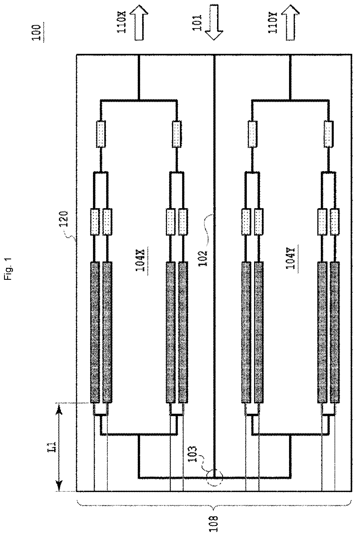
[0061]FIG. 6 is a chip plan view of an IQ optical modulator according to Example 1. The IQ optical modulator 600 of Example 1 is a single-polarization IQ optical modulator that has an I-channel optical modulation region 604a and a Q-channel optical modulation region 604b that form child MZMs of a single nest-type MZM on the chip 620.

[0062]The IQ optical modulator 600 of FIG. 6 is an IQ optical modulator including a nest-type MZ optical waveguide that forms the I channel optical modulation region 604a and the Q channel optical modulation region 604b as a child MZM. The end portions of the input optical waveguide 601 of the light input part and the output optical waveguide 610 of the light output part are located on the same edge face (right edge face in FIG. 6) of the chip 620.

[0063]On the other hand, an optical waveguide connecting a first optical combiner 607b that is an optical combiner of a child MZM, for example, on the Q-channel side, and a second optical combiner 609 that is a...

example 2

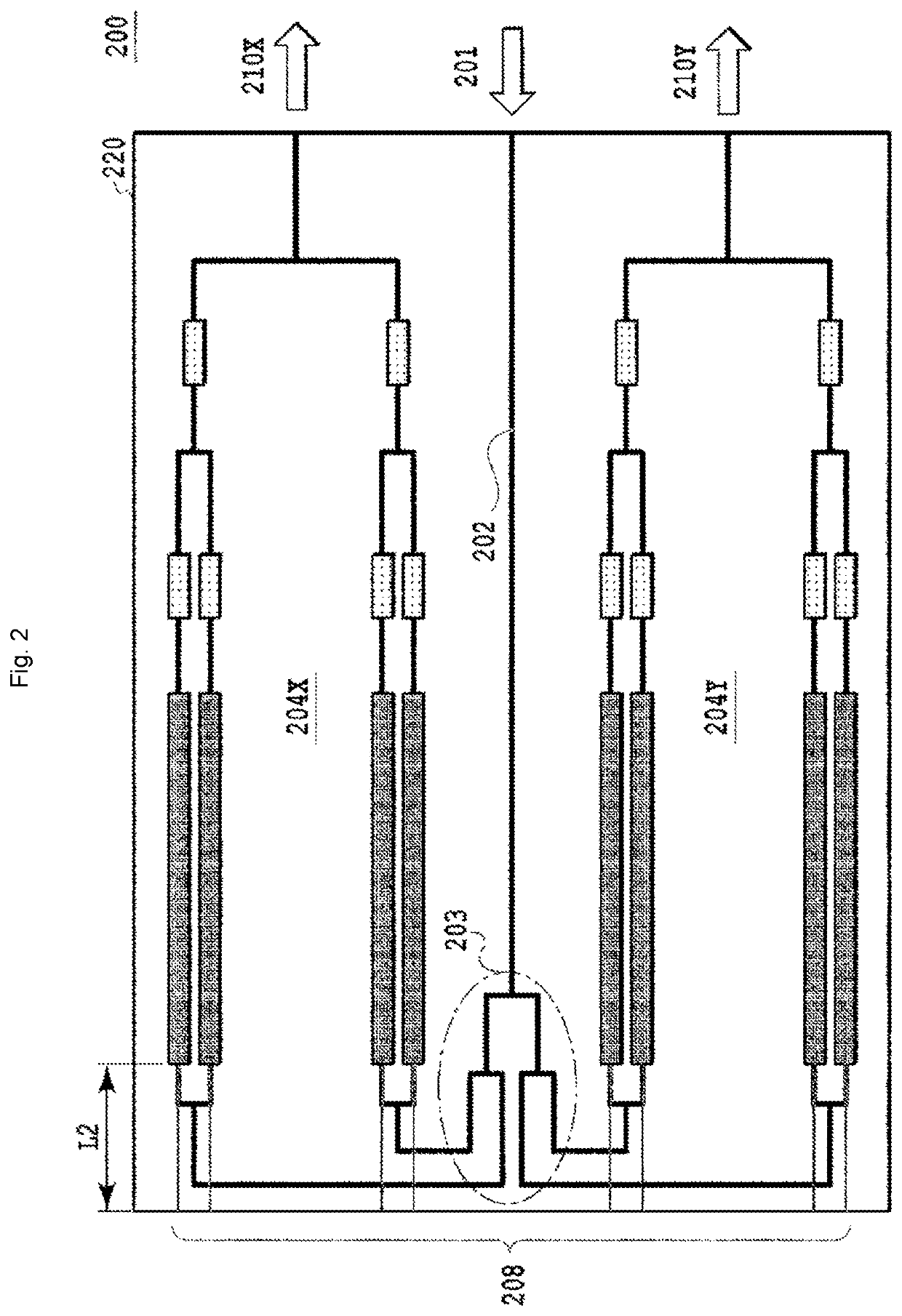
[0069]An IQ optical modulator 700 of Example 2 illustrated in FIG. 7 is a polarization-multiplexed IQ optical modulator in which the two IQ optical modulators 600 of Example 1 are integrated in parallel on the chip 720 for X and Y polarization channels to form a polarization-multiplexed IQ optical modulator. The configuration in which total four MZ modulators are integrated on the chip 720 is used in actual polarization-combined systems.

[0070]In the polarization-multiplexed IQ optical modulator 700 of FIG. 7, light input from the input optical waveguide 701 is divided by an XY polarization divider 730 into X and Y polarization channels, and via the optical cross waveguides 702X and 702Y, the light is drawn between the IQ channel optical modulation regions 704XI and 704XQ or 704YI and 704YQ of each polarization channel, and thereafter the light is divided, folded back, and modulated. The modulated light is then combined by each polarization channel, and finally output as X-polarizati...

example 3

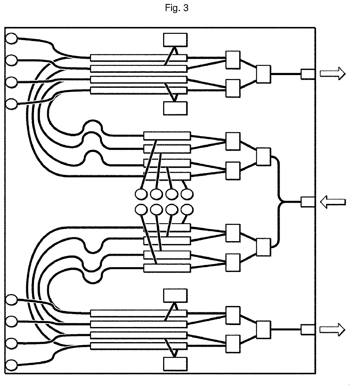
[0071]FIG. 8 illustrates a polarization-multiplexed IQ optical modulator 800 according to Example 3. The IQ optical modulator 800 according to Example 3, in the configuration of the polarization-multiplexed IQ optical modulator 700 according to Example 2, the second optical dividers 806XI and 806XQ (with respect to the Y-polarization side, element symbols in FIG. 8 are omitted) that are the optical dividers of the child MZMs are also provided between the I-channel optical modulation region and the Q-channel optical modulation region, and the light propagation direction in the second optical dividers and the light propagation direction in the optical modulation regions are opposite (180°).

[0072]With the configuration according to Example 3, the DC phase adjusters 808XIa, 808XQa, 808XIb, and 808XQb (with respect to the Y-polarization side, element symbols in FIG. 8 are omitted) provided in the waveguides of the child MZMs can be formed before the turning position, so that the DC phase...


PUM

PropertyMeasurementUnit
speedaaaaaaaaaa
optical phaseaaaaaaaaaa
temperature fluctuationaaaaaaaaaa

Abstract

Provided is an IQ optical modulator including a nest-type MZ optical waveguide having optical modulation regions of I channel and Q channel End portions of an input optical waveguide and an output optical waveguide of the IQ optical modulator are located on a same edge face of a chip of the IQ optical modulator, an optical cross waveguide is included in which an optical waveguide between a first optical combiner and a second optical combiner of the nest-type MZ optical waveguide and the input optical waveguide cross each other, a first optical divider is provided between the I-channel optical modulation region and the Q-channel optical modulation region, and a light propagation direction in the first optical divider and a light propagation direction in the optical modulation regions are opposite to each other.

Description

TECHNICAL FIELD[0001]The present disclosure relates to an IQ optical modulator capable of high speed and wide wavelength band operation.BACKGROUND ART[0002]With the increased capacity of optical communication systems, high-speed optical modulators supporting advanced optical modulation schemes are required. In particular, multilevel optical modulators using digital coherent technologies play a major role in enabling high-capacity transceivers having a capacity over 100 Gbps. In these multilevel optical modulators, in order to add independent signals to the amplitude and phase of light, optical modulators (MZM) capable of zero-chirp drive are built in parallel in multiple stages, and the optical modulators (MZM) includes a Mach-Zehnder interference-type optical waveguide (MZ optical waveguide) which divides an optical input into two arms, and then combines and interference-outputs these divided lights after phase shift.[0003]A typical polarization-multiplexed IQ optical modulator tha...

Claims


Application Information

Patent Timeline
Patent Type & Authority Applications(United States)
IPC IPC(8): G02F1/225G02F1/21
CPCG02F1/2255G02F1/212G02F1/225G02B6/29344
Inventor OGISO, YOSHIHIROOZAKI, JOSUKEHASHIZUME, YASUAKIISHIKAWA, MITSUTERUNUNOYA, NOBUHIRO
Owner NIPPON TELEGRAPH & TELEPHONE CORP
Why Eureka
Try Eureka