Logarithmic linear variable gain CMOS amplifier

a cmos amplifier and linear variable technology, applied in amplifiers, dc-amplifiers with dc-coupled stages, analog and hybrid computing, etc., can solve the problems of bias current affecting the bandwith and linearity of the amplifier, and achieve the effect of adding complexity

Active Publication Date: 2010-06-15
STMICROELECTRONICS SRL
View PDF7 Cites 7 Cited by
  • Summary
  • Abstract
  • Description
  • Claims
  • Application Information

AI Technical Summary

Problems solved by technology

However, the variation of the bias current also affects the bandwith and the linearity of the amplifier.

Method used


Image

  • Logarithmic linear variable gain CMOS amplifier
  • Logarithmic linear variable gain CMOS amplifier
  • Logarithmic linear variable gain CMOS amplifier

Examples


Embodiment Construction

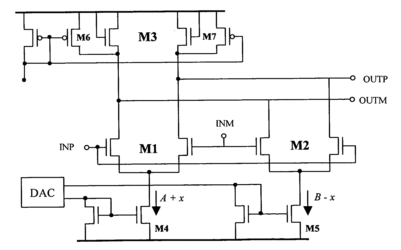
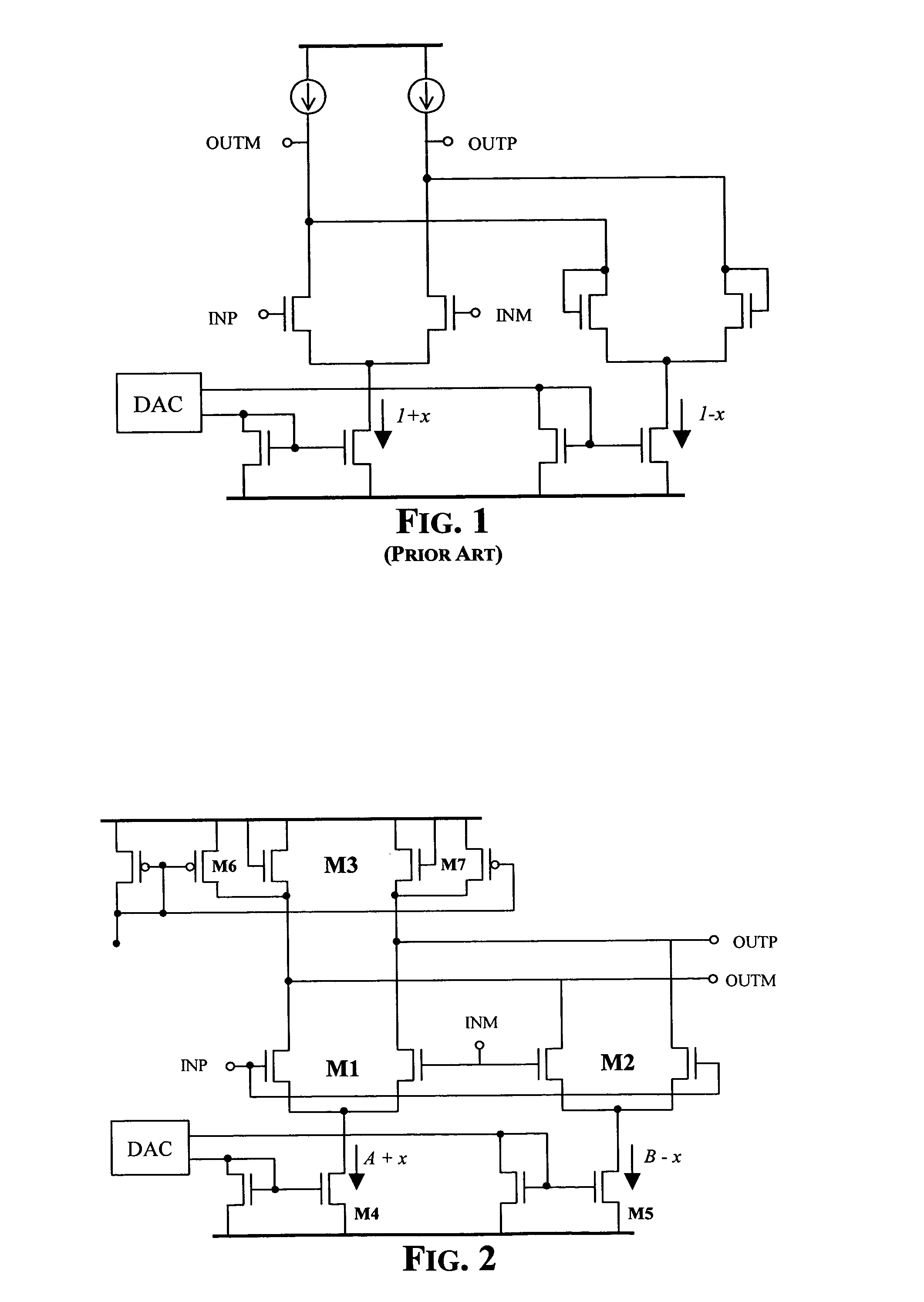
[0015]As depicted in FIG. 2, the two differential transistor pairs M1 and M2, sharing the same diode-connected load transistors M3, are cross connected to the inpuit nodes INP and INM of the amplifier according to an essential feature of the circuit of the present invention.

[0016]The transconductance of the first input differential pair of transistors M1 is gm1, the transconductance of the second input differential pair of transistors M2 is gm2, and the transconductance of the diode-connected load transistors M3 is gm3. It may be demonstrated that the gain of the amplifier is given by the following equation:

[0017]Gain=gm1-gm2gm3=K1·I1-K2·I2K3·I3(2)

where Ki is the transistor's gain constant proportional its aspect ratio W / L; I1, I2 and I3 are the respective bias currents of M1, M2 and M3; and the bandwith is given by the following equation:

[0018]Bandwidth≅K3·I3π·Cout(3)

wherein Cout is the capacitance of the output node, referred to the virtual ground node of the circuit.
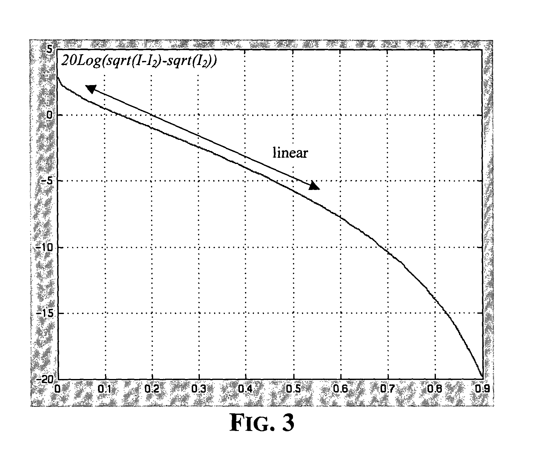
[0019]Customa...


PUM


Abstract

A logarithmic linear variable gain CMOS amplifier includes first and second differential pairs of transistors forming a differential input, with each differential pair of transistors including a common source node. A pair of diode-connected load transistors is connected to the first and second differential pairs of transistors, and a third differential pair of transistors is connected to the pair of diode-connected load transistors. The third differential pair of transistors include respective gates connected together and in parallel to gates of the first and second differential pairs of transistors. First and second current mirrors are respectively connected to the common source nodes of the first and second differential pairs of transistors for programmably injecting respective bias currents thereto, with a sum of the respective bias currents remaining constant.

Description

FIELD OF THE INVENTION[0001]The present invention relates in general to integrated analog circuits, and in particular, to an integrated logarithmic linear variable gain CMOS amplifier.BACKGROUND OF THE INVENTION[0002]State of the art logarithmic linear amplifiers are based on a circuit structure as illustrated in FIG. 1. Such a structure is disclosed in U.S. Patent Application No. 2002 / 0048109. The gain of these amplifiers commonly use two stages for increasing the gain range, which is given by the following equation:[0003]Gain=1+x1-x(1)[0004]The linear logarithmic gain (dB gain) variation range of the function is relatively restricted. Generally, the value of x of the gain expression for remaining substantially in the linear dB gain variation range is limited to −0.7<x<0.7.[0005]The variation of the bias current in a transistor notably alters its transconductance, thus obtaining the desired behavior of the circuit according to equation 1. However, the variation of the bias cu...

Claims


Application Information

Patent Timeline
Patent Type & Authority Patents(United States)
IPC IPC(8): G06G7/24H03G7/00H03G7/06
CPCH03G7/06H03G7/001
Inventor GAETA, MARCOBOLLATI, GIACOMINOBONGIORNI, MARCO
Owner STMICROELECTRONICS SRL
Why Eureka
Try Eureka