Liquid crystal display device and driving method used in same

a technology of liquid crystal display and driving method, which is applied in the direction of static indicating devices, instruments, optics, etc., can solve the problems of over-the-counter liquid crystal display device, difficult to provide a low-priced product, and increase the number of components and fabricating processes, so as to achieve bright display, wide color reproducibility, and simplify the configuration of the liquid crystal display panel.

Inactive Publication Date: 2010-07-13
NEC LCD TECH CORP
View PDF12 Cites 7 Cited by
  • Summary
  • Abstract
  • Description
  • Claims
  • Application Information

AI Technical Summary

Benefits of technology

[0017]In view of the above, it is an object of the present invention to provide a liquid crystal display device which is capable of reducing the number of components and fabricating processes and making bright a display screen even at time of a transmissive display operation and making simple configurations of a data signal, and a method of driving the liquid crystal display device.
[0057]With the above configuration, the coloring layer corresponding to each of the three colors of R, G, and B is formed in part of the corresponding pixel cell and, therefore, at time of the transmissive display operation, wide color reproducibility can be achieved and, at time of the reflective display operation, bright display can be realized.
[0058]With another configuration as above, the data signal distributing unit distributes and inputs one kind of data signal, as a sub-pixel data signal, to the data electrode selected based on a selecting signal corresponding to the successive additive color mixture or juxtapositional additive color mixture process and, therefore, it is not necessary to mount a circuit to generate a data signal corresponding to the FS driving, transmissive display, and reflective display, which enables simplification of the configurations of the liquid crystal display panel. Moreover, the semi-transmissive light reflecting plate is provided outside of the liquid crystal panel and on a side opposite to a viewer side and, therefore, configurations of the liquid crystal panel can be simplified.
[0059]With still another configuration as above, the semi-transmissive light reflecting plate is formed inside of the liquid crystal panel and has a transmissive region which allows colored light having entered from the light source to be transmitted in every sub-pixel and to output the colored light to a viewer side and a reflective region which reflects light having entered through the coloring layer from the viewer side and outputs the colored light through the same coloring layer to the viewer side, wherein the reflective region is formed in a manner to correspond to the coloring layer and, therefore, at time of the reflective display operation, no parallax occurs and the transmissive region is not influenced at all by a color of the coloring layer which allows the coloring layer to be designed independently, thus enabling easy designing of the liquid crystal display device. Also, at the time of the transmissive display operation, light fed from the light source passes only through the transmissive region where no coloring layer is provided and, therefore, no light is absorbed by the coloring layer to allow all light to pass through the transmissived region, which makes it possible to make the most of high color purity of the light emitting element itself and which enables bright display and wide color reproducibility in the liquid crystal panel. As a result, luminance of the light source can be decreased and power consumption can be greatly reduced.

Problems solved by technology

However, the above conventional liquid crystal display device has following problems.
The first problem is that, not only mounting of the upper-side retardation plate 3 and lower-side retardation plate 5 but also a process of forming the reflecting plate / coloring layer 11 is required, which causes the number of components and fabricating processes to be increased and makes it difficult to provide a low-priced product.
The second problem is that, at the time of the transmissive display operation, a display screen is dark.
The third problem is that three kinds of data signals to correspond to the FS driving, transmissive display, and reflective display are necessary, which causes configurations to be complicated.
The reason for the occurrence of the first problem is that precise patterning on the reflecting plate / coloring layer 11 is required, which causes fabricating processes to increase and yields to be reduced.
Moreover, in the case of using a mirror reflecting plate as the reflecting plate, a dark display screen appears when the display is seen from a direction other than a direction of specular reflection of incident light, which makes it difficult to see the display fully in some cases.
To solve this problem, formation of bumps and dips to reduce the specularly reflected light component by using a resin or a like or insertion of a diffusive sheet in which tiny transparent particles are dispersed between the upper-side polarizer 4 and lower-side polarizer 6 and between the upper-side substrate 1 and lower-side substrate 2 is required, which increases further the number of fabricating processes and decreases cost-performance.
In particular, as a material for the upper-side retardation plate 3 and lower-side retardation plate 5, a norbornene transparent resin having a lower wavelength dispersion characteristic is used, however, the material is expensive, which makes it difficult to lower the price of the liquid crystal display device.
Therefore, in order to obtain luminance being equivalent to luminance obtained by the FS driving operation in which only the transmissive driving operation is performed without using the coloring layer 12, the luminance needs to be higher at least two times to three times than the luminance of the backlight and, as a result, a problem arises that power consumption is greatly increased.
Also, even when each pixel cell is driven simultaneously, a signal for each pixel cell needs to be generated, which causes the configurations of the liquid crystal display device to be more complicated.
In this case, control of a film thickness is difficult and there is a limit to a degree (for example, 0.3 mm) to which a film is made thin.
Due to this, a problem arises that a decrease in visual recognition caused by the occurrence of parallax and / or color mixture occurs.
Moreover, specific gravity of a glass substrate is comparatively high and it is, therefore, difficult to make the liquid crystal display device lightweight and thin to a degree to which a mobile device such as a portable phone or PDA (Personal Digital Assistants) requires.
Furthermore, the liquid crystal display device disclosed in the above Patent Reference 1, since it has configurations similar to those of the liquid crystal display device shown in FIG. 17, has the same problems as described above.

Method used


Image

  • Liquid crystal display device and driving method used in same
  • Liquid crystal display device and driving method used in same
  • Liquid crystal display device and driving method used in same

Examples


first embodiment

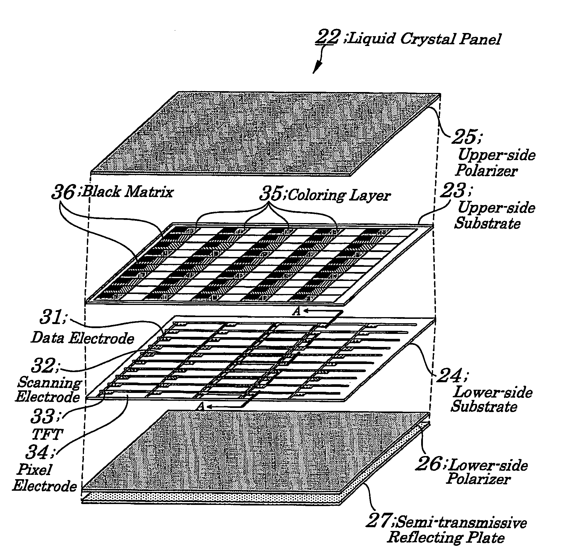
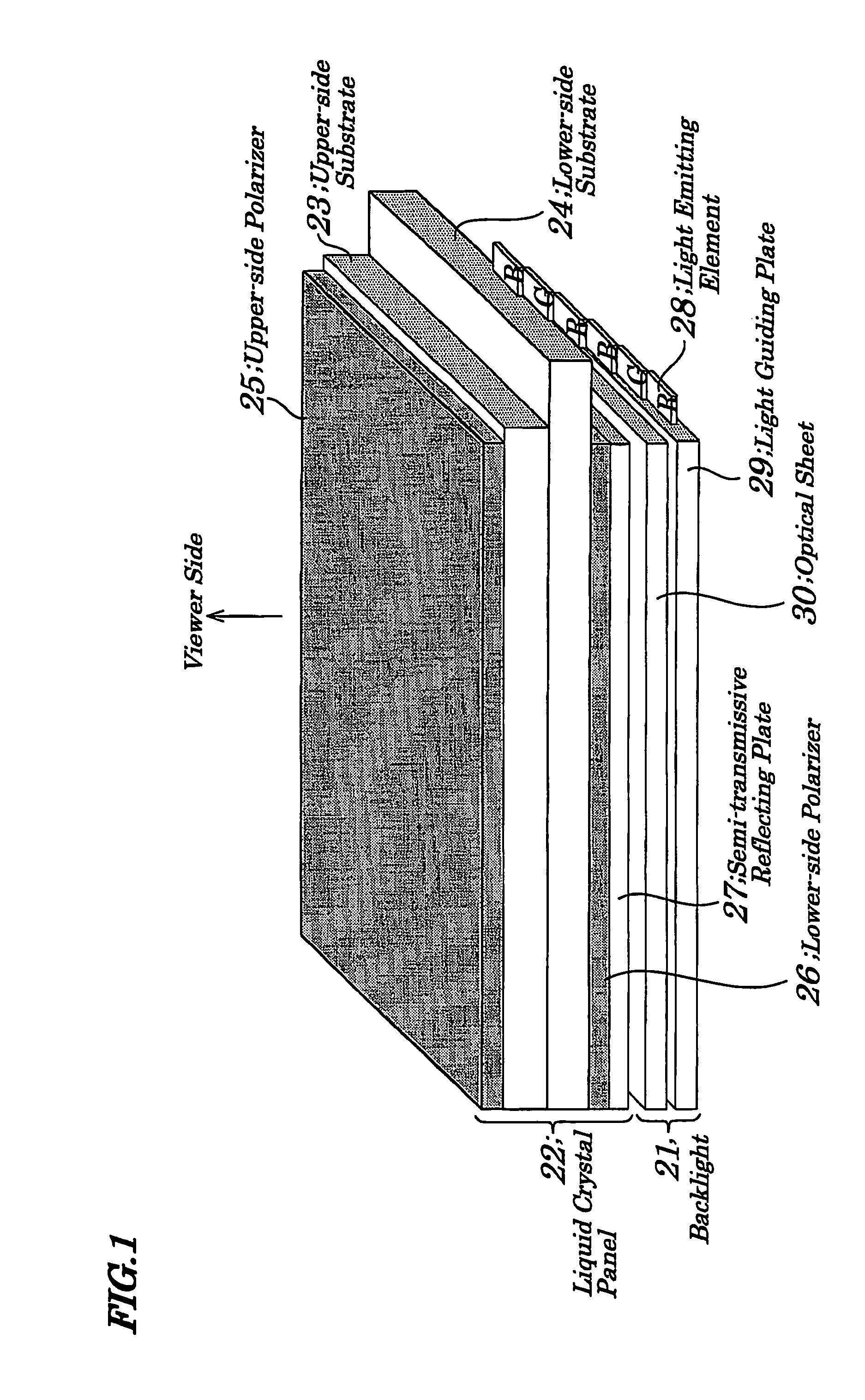
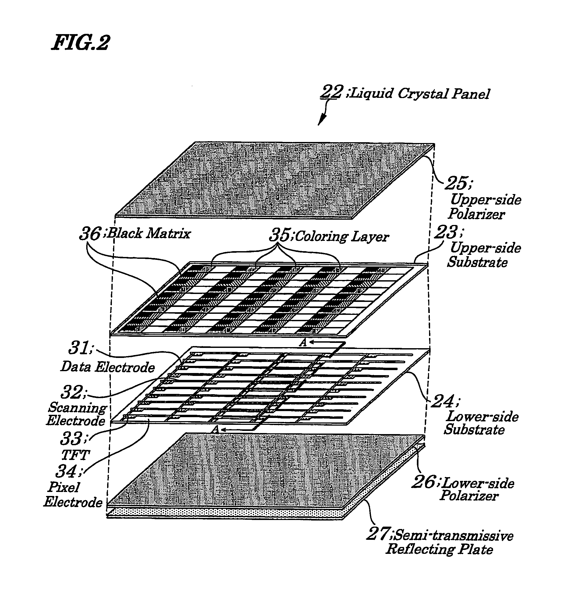
[0081]FIG. 1 is a perspective view showing configurations of main components making up a liquid crystal display device of a first embodiment of the present invention. The liquid crystal display device of the first embodiment, as shown in FIG. 1, is made up of a backlight 21 and a liquid crystal panel 22. The liquid crystal panel 22 includes an upper-side substrate 23, a lower-side substrate 24, an upper-side polarizer 25, a lower-side polarizer 26, and a semi-transmissive reflecting plate 27. The upper-side substrate 23 and lower-side substrate 24 are made of a transparent substrate such as a glass, a transparent resin, or a like. The upper-side substrate 23 is formed on a visually-recognized side (viewer side) and the lower-side substrate 24 is formed on the backlight 21 side being opposite to the viewer side. The upper-side polarizer 25 is bonded to the viewer side of the upper-side substrate 23 and the lower-side polarizer 26 and the semi-transmissive reflecting plate 27 are bond...

second embodiment

[0100]FIG. 12 is an exploded perspective view showing configurations of main components making up a liquid crystal display device according to a second embodiment of the present invention and same reference numbers are assigned to components having the same function of those shown in FIG. 2 of the first embodiment. A liquid crystal panel 22A of the second embodiment, as shown in FIG. 12, has plurality kinds of coloring layers 35A and an element of black matrix 36A formed on each of TFTs 33 on a lower-side substrate 24 and of a COT (Color Filter on TFT) structure. Configurations other than the above are the same as shown in FIG. 2.

[0101]FIG. 13 is a cross-sectional view of the liquid crystal panel of FIG. 12 taken along a line A-A. As shown in FIG. 13, a liquid crystal layer 37 is sandwiched between the upper-side substrate 23 and lower-side substrate 24 and, on the coloring layer 35A and elements of a black matrix 36A on the lower-side substrate 24 is stacked an over coat 38A in lay...

third embodiment

[0104]FIG. 14 is a perspective view showing configurations of main components making up a liquid crystal display device according to the third embodiment of the present invention. In a liquid crystal display panel 22B of the third embodiment, as shown in FIG. 14, the liquid crystal panel 22B is provided which has configurations being different from those of the liquid crystal panel 22 shown in FIG. 1. In the liquid crystal panel 22B, a semi-transmissive reflecting plate 27 formed in the liquid crystal panel 22 of the first embodiment is omitted.

[0105]FIG. 15 is an exploded perspective view showing configurations of main components making up the liquid crystal panel 22B shown in FIG. 14. In the liquid crystal panel 22B, as shown in FIG. 15, between an upper-side polarizer 25 and an upper-side substrate 23 is interposed an upper-side retardation plate 51 and between a lower-side polarizer 26 and a lower-side substrate 24 is interposed a lower-side retardation plate 52.

[0106]FIG. 16 is...


PUM

PropertyMeasurementUnit
thicknessaaaaaaaaaa
thicknessaaaaaaaaaa
coloraaaaaaaaaa

Abstract

A liquid crystal display device is provided which is capable of reducing a number of components and fabricating processes and of realizing a bright display even at time of a transmissive display and of simplifying configurations of a data signal. Transistors are controlled ON / OFF based on selecting signals input to selecting signal lines and a one kind of data signal input from data lines distributed and supplied, as a sub-pixel data, to a data electrode selected based on selecting signals corresponding to a successive additive color mixture or juxtapositional additive color mixture process. At time of the transmissive display operation, data electrodes corresponding to three sub-pixels making up each pixel are simultaneously selected and, at time of the reflective display operation, data electrodes selected based on selecting signal corresponding to the juxtapositional additive color mixture.

Description

BACKGROUND OF THE INVENTION[0001]1. Field of the Invention[0002]The present invention relates to a liquid crystal display device and a driving method to be used in the liquid crystal display device and more particularly to the liquid crystal display device suitably used when either of transmissive display or reflective display is selected depending on variations in environments for using the liquid crystal display device and the driving method to be used in the liquid crystal display device.[0003]The present application claims priority of Japanese Patent Application No. 2005-044855 filed on Feb. 21, 2005, which is hereby incorporated by reference.[0004]2. Description of the Related Art[0005]A liquid crystal display device is classified into two types of devices, one being a transmissive-type liquid crystal display device in which light emitted from an embedded backlight is transmitted through a liquid crystal panel to achieve displaying and another being a reflective-type liquid cry...

Claims


Application Information

Patent Timeline
Patent Type & Authority Patents(United States)
IPC IPC(8): G09G3/36G02F1/1335
CPCG09G3/3406G09G3/3688G09G3/3648G09G2300/0456G09G2310/0235G09G2310/0297G09G2360/144G02F2001/133557G02F1/133557G09G3/36G09G5/02G02F1/1335
Inventor NAKA, KEN-ICHIROUSAKAMOTO, MICHIAKI
Owner NEC LCD TECH CORP
Why Eureka
Try Eureka