Automatic defect repair system

a defect repair and automatic technology, applied in the field of flat panel displays, can solve the problems of affecting the electrical and/or optical performance of the final lcd product, mask problems, over or under etching, and unavoidable defects, and achieve the effect of reducing the amount of operator time and efficient decision-making

Active Publication Date: 2010-07-20
ORBOTECH LTD
View PDF10 Cites 23 Cited by
  • Summary
  • Abstract
  • Description
  • Claims
  • Application Information

AI Technical Summary

Benefits of technology

[0017]Defect classification, repair classification, and repair macro generation are based on an open architecture and can address any number of use-cases through the use of multi-tiered classifiers, and thus a wide variety of panel designs may be repaired within a single repair tool. In particular, the method of the present invention includes recognition that automatic repair depends on defect classification, and that a multi-tiered set of classifiers, e.g., defect classifier, repair classifier, enables an efficient decision-making repair process with capability for customization.
[0018]The present invention is adapted to extend the rule-based classifier to include statistical learning (both online & batch) and active learning, in the context of a supporting database of defects and associated tools. Thus, the classifiers and recipe rules may be automatically or semi-automatically improved over time, incorporating lessons learned by operators while judging defect or repair needs. Accordingly, the defect repair system of the present invention is adapted to reduce the amount of operator time spent per tool, but also recognizes that there must be latitude in the tool operation for human intervention.

Problems solved by technology

During each of these stages and at various steps within each stage, many production defects may occur that may affect the electrical and / or optical performance of the final LCD product.
Other defects include mask problems, over or under etching, etc.
Even though the TFT deposition processes are tightly controlled, defect occurrence is unavoidable.
This limits the product yield and adversely effects production costs.
Commonly AOI and AC systems provide defect coordinates; they do not provide high resolution images required to classify defects as killer, reparable or just imperfections not affecting the TFT array performance (so called process defects).
Sometimes a single plate has numerous and different kinds of defects, and the operator prioritizes the order in which the repairs are made.
However, due to variations in image quality, the operator may mistakenly identify the defect type or bin inconsistently or with ambiguity.
A further challenge arises at the time of factory start-up, when the available classification data may be scarce or not accurate.
Since the publication of the above article, LCD panel fabrication has grown in complexity with the increase in use case for LCD panels ranging from computer laptop screens to computer monitors to television screens.

Method used


Image

  • Automatic defect repair system
  • Automatic defect repair system
  • Automatic defect repair system

Examples


Embodiment Construction

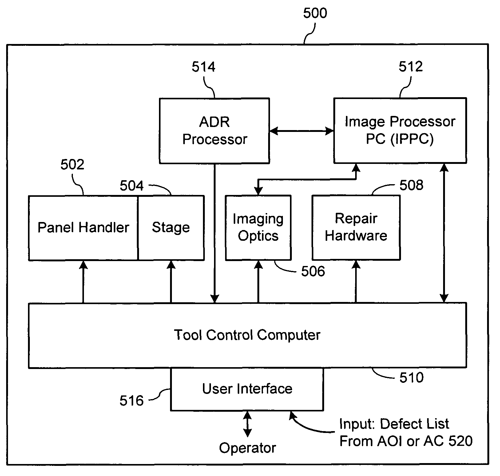
[0036]FIG. 5 is a functional block diagram of a LCD array repair tool 500, in accordance with one exemplary embodiment of the present invention. Exemplary array repair tool 500 is shown as including, in part, a panel handler 502, a stage 504 to move the sample LCD panel (not shown) into, within, and out of the tool; imaging optics 506 to capture images; repair hardware 508 to make defect repairs; a tool controller 510 adapted to control the hardware used to repair defects, an image processing computer 512 (IPPC) that processes the defect images, and an automatic defect repair (ADR) processor 514. Human operators control the tool through the graphical user interface 516 (GUI). In some embodiments, ADR processor 514 may be a part of or disposed in image processing computer 512. In yet other embodiments, ADR processor 514 may be a part of or disposed in embedded tool control computer 510. Furthermore, tool control computer 510 may be an embedded computer.

[0037]Imaging optics 506 typica...


PUM


Abstract

A repair system for flat panel display (FPD) substrates performs a number of operations, such as automatic image capture and processing, automatic defect classification, automatic repair classification, and repair macro (instruction) generation software. Defect classification, repair classification, and repair macro generation are based on an open architecture and can address any number of use-cases through the use of multi-tiered classifiers, and thus a wide variety of panel designs may be repaired within a single repair tool. The multi-tiered set of classifiers, e.g., defect classifier, repair classifier, enables an efficient decision-making repair process with capability for customization. The multi-tiered classifiers are optionally extended to support statistical learning (both online & batch) and active learning, in the context of a supporting database of defects and associated tools. The classifiers and recipe rules may be automatically or semi-automatically improved over time, incorporating lessons learned by operators while judging defect or repair needs.

Description

CROSS-REFERENCES TO RELATED APPLICATIONS[0001]The present application claims priority under 35 U.S.C. 119(e) from application Ser. No. 60 / 646,111, filed Jan. 21, 2005 entitled “Automatic Defect Repair System”, the content of which is incorporated herein by reference in its entirety.BACKGROUND OF THE INVENTION[0002]The present invention relates to the flat panel displays based on liquid crystal display (LCD) and other related display technologies such as organic light emitting devices (OLED), and more particularly to the inspection of components formed on such displays.[0003]During the manufacturing of LC displays, large clear plates of thin glass are used as a substrate for the deposition of thin film transistor (TFT) arrays. Usually, several independent TFT arrays are contained within one glass substrate plate and are often referred to as TFT panels. Alternatively, an active matrix LCD, or AMCLD, covers the class of displays utilizing a transistor or diode at every subpixel, and th...

Claims


Application Information

Patent Timeline
Patent Type & Authority Patents(United States)
IPC IPC(8): G06F19/00G06V10/764
CPCG02F1/1309G02F1/136259G06K9/628G09G3/006G06T7/001G02F2001/136263G09G2330/08G06T2207/10024G06T2207/30121G02F1/136263G06V10/764G06F18/2431G02F1/13
Inventor GALLARDA, HARRYBARNES, STEVENSRINIVASAN, LAKSHMANWANG, WAYNE
Owner ORBOTECH LTD
Why Eureka
Try Eureka