Display

a display and display technology, applied in the field of display, can solve the problems of disadvantageous input of on-state at unintentional timing, shift register circuit disadvantageous output, and unintentional timing of /b>, etc., to suppress fluctuation, suppress destabilization of operations, and suppress occurrence

Inactive Publication Date: 2010-08-17
JAPAN DISPLAY WEST
View PDF18 Cites 5 Cited by
  • Summary
  • Abstract
  • Description
  • Claims
  • Application Information

AI Technical Summary

Benefits of technology

[0018]In the display according to the aforementioned aspect, both of the first shift register circuit portion and the second shift register circuit portion preferably include the reset transistors. According to this structure, the display can fix both of the first and second shift signals output from the first and second shift register circuit portions respectively to the second voltage supply source not turning on the transistors of the logic composition circuit portion with the reset transistors. Thus, the display can hold both of two transistors of the logic composition circuit portion in OFF-states when inputting the first and second shift signals in the gates of the two transistors of the logic composition circuit portion respectively and employing a signal output through the two transistors as the shift output signal obtained by logically compositing the first and second shift signals with each other. Therefore, the display can more reliably inhibit the logic composition circuit portion from outputting a signal to the gate line or the drain line at unintentional timing.
[0033]In the display according to the aforementioned aspect, transistors constituting the first shift register circuit portion and the second shift register circuit portion and the transistors constituting the logic composition circuit portion as well as the reset transistor are preferably of a first conductive type. According to this structure, the numbers of ion implantation steps and ion implantation masks for forming these transistors can be reduced as compared with a case of forming the transistors constituting the first shift register circuit portion, the second shift register circuit portion and the logic composition circuit portion and the reset transistor by transistors having two conductive types, i.e., first and second conductive types. Thus, complication of a manufacturing process as well as the manufacturing cost can be suppressed.

Problems solved by technology

Thus, the transistors NT510 to NT512 of the horizontal switch 1100 having the gates connected to the nodes ND504 may disadvantageously enter ON-states at unintentional timing.
In this case, the shift register circuit disadvantageously outputs the video signals from the video signal line Video to the drain lines through the ON-state transistors NT510 to NT512 at unintentional timing.

Method used


Image

  • Display
  • Display
  • Display

Examples


first embodiment

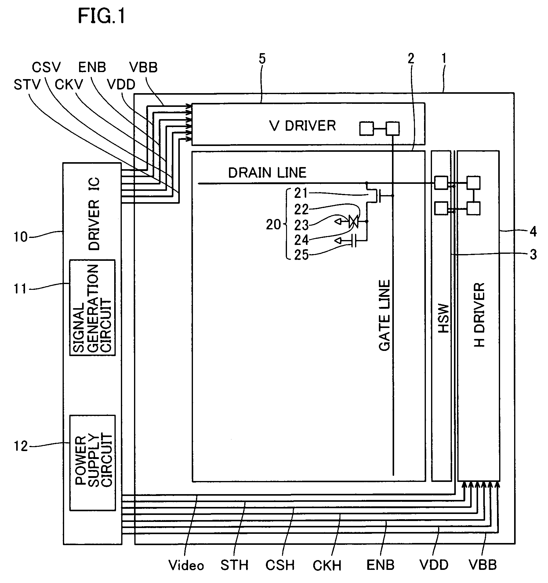
[0055]FIG. 1 is a plan view showing a liquid crystal display according to a first embodiment of the present invention. Referring to FIG. 1, a display portion 2 is provided on a substrate 1 in the liquid crystal display according to the first embodiment. Pixels 20 are arranged on the display portion 2 in the form of a matrix. FIG. 1 shows only one of the pixels 20, in order to simplify the illustration. Each pixel 20 is constituted of an n-channel transistor 21 (hereinafter referred to as a transistor 21), a pixel electrode 22, a common electrode 23, opposed to the pixel electrode 22, common to each pixel 20, a liquid crystal 24 held between the pixel electrode 22 and the common electrode 23 and a subsidiary capacitor 25. The source of the transistor 21 is connected to the pixel electrode 22 and the subsidiary capacitor 25, while the drain thereof is connected to a drain line. The gate of the transistor 21 is connected to a gate line.

[0056]Horizontal switches (HSW) 3 and an H driver ...

second embodiment

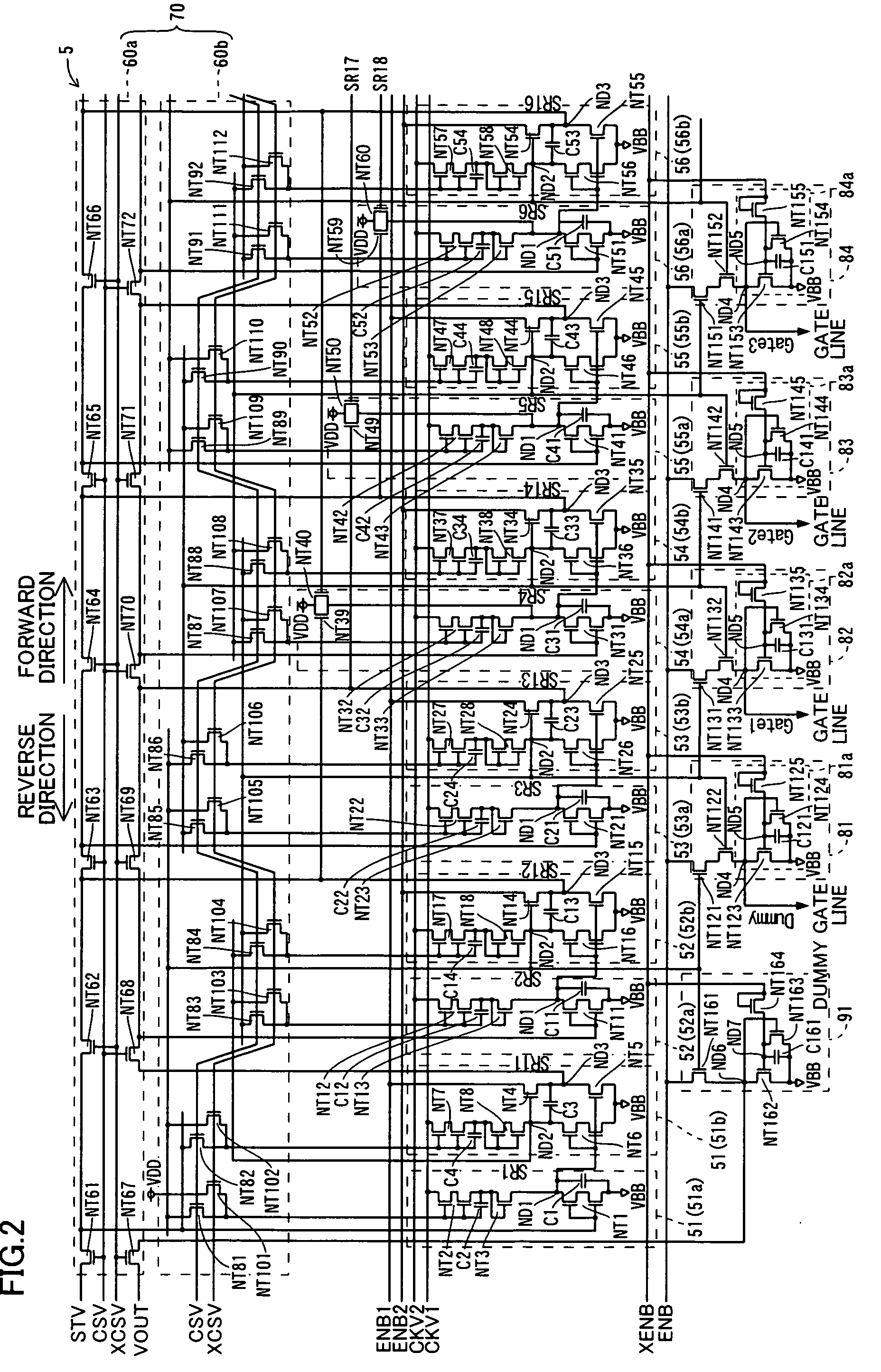
[0160]Referring to FIGS. 4 and 5, a V driver 5a similar to the V driver 5 according to the aforementioned first embodiment is constituted of p-channel transistors in a liquid crystal display according to a second embodiment of the present invention.

[0161]Referring to FIG. 4, a display portion 2a is provided on a substrate 1a in the liquid crystal display according to the second embodiment. Pixels 20a are arranged on the display portion 2a in the form of a matrix. FIG. 4 shows only one of the pixels 20a, in order to simplify the illustration. Each pixel 20a is constituted of a p-channel transistor 21a (hereinafter referred to as a transistor 21a), a pixel electrode 22a, a common electrode 23a common to each pixel 20a opposed to the pixel electrode 22a, a liquid crystal 24a held between the pixel electrode 22a and the common electrode 23a and a subsidiary capacitor 25a. The source of the transistor 21a is connected to a drain line, while the drain thereof is connected to the pixel ele...

third embodiment

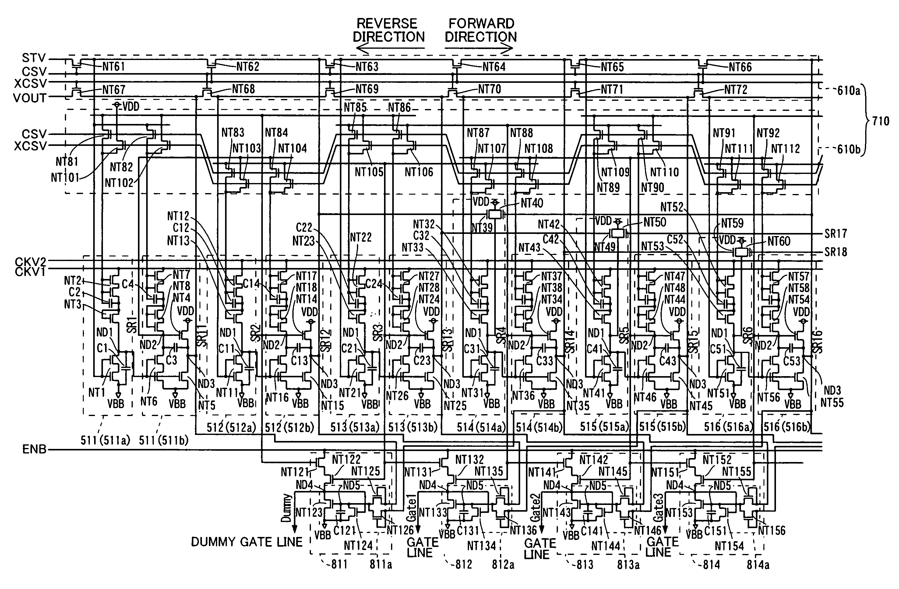
[0186]Referring to FIG. 7, a liquid crystal display according to a third embodiment of the present invention supplies a higher voltage supply source VDD to the drains of transistors connected to nodes outputting output signals while holding shift output signals output from logic composition circuit portions in states fixed to low levels through the output signals from the shift register circuit portions in a structure similar to that of the aforementioned first embodiment.

[0187]As shown in FIG. 7, a V driver of the liquid crystal display according to the third embodiment is provided with a plurality of stages of shift register circuit portions 511 to 516, a scanning direction switching circuit portion 710 formed by an output signal input switching circuit portion 610a and a shift signal input switching circuit portion 610b and a plurality of stages of logic composition circuit portions 811 to 814. The shift register circuit portions 512 to 516 are examples of the “first shift regist...


PUM


Abstract

A display capable of inhibiting a logic composition circuit from outputting a signal to a gate line or a drain line at unintentional timing is obtained. In this display, at least either a first shift register circuit portion or a second shift register circuit portion includes a reset transistor for resetting the voltage supply source of a node outputting a first shift signal or a second shift signal to a second voltage supply source not turning on transistors of a logic composition circuit portion in response to an output signal received from a shift register circuit portion precedent thereto by at least two stages with respect to a scanning direction.

Description

BACKGROUND OF THE INVENTION[0001]1. Field of the Invention[0002]The present invention relates to a display, and more particularly, it relates to a display comprising a shift register circuit.CROSS-REFERENCE TO RELATED APPLICATIONS[0003]The priority application number JP2005-96631 upon which this patent application is based is hereby incorporated by reference.[0004]2. Description of the Background Art[0005]A display comprising a shift register circuit is known in general, as disclosed in Japanese Patent Laying-Open No. 2005-17973, for example.[0006]FIG. 18 is a circuit diagram for illustrating the circuit structure of a shift register circuit driving drain lines of the exemplary conventional display disclosed in the aforementioned Japanese Patent Laying-Open No. 2005-17973. Referring to FIG. 18, the shift register circuit driving the drain lines of the exemplary conventional display is provided with a plurality of stages of shift register circuit portions 1001 to 1003. The first-stag...

Claims


Application Information

Patent Timeline
Patent Type & Authority Patents(United States)
IPC IPC(8): G09G3/36
CPCG11C19/00G11C19/28B26B11/00B26B3/02
Inventor HORIBATA, HIROYUKISENDA, MICHIRU
Owner JAPAN DISPLAY WEST
Why Eureka
Try Eureka