

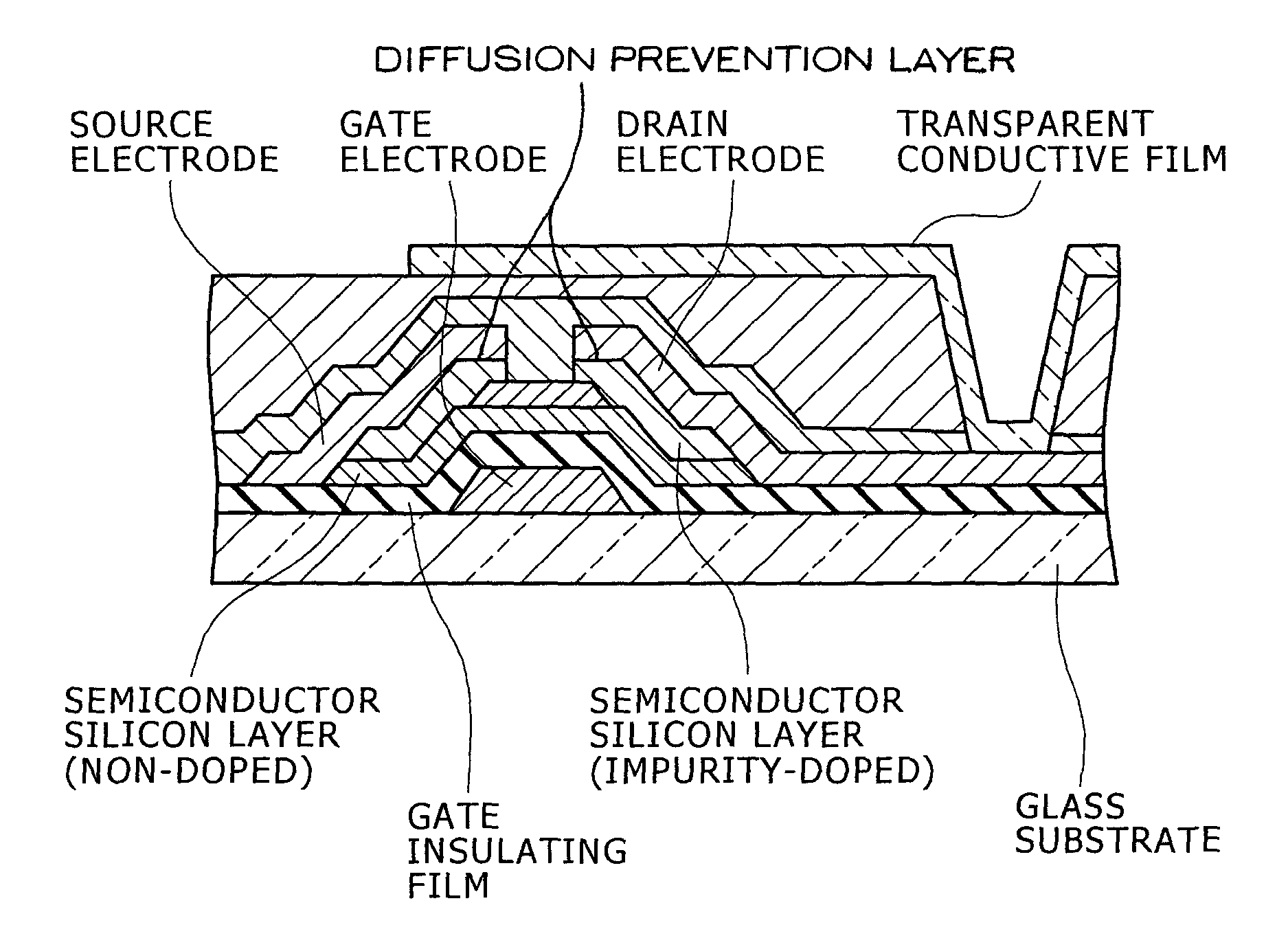
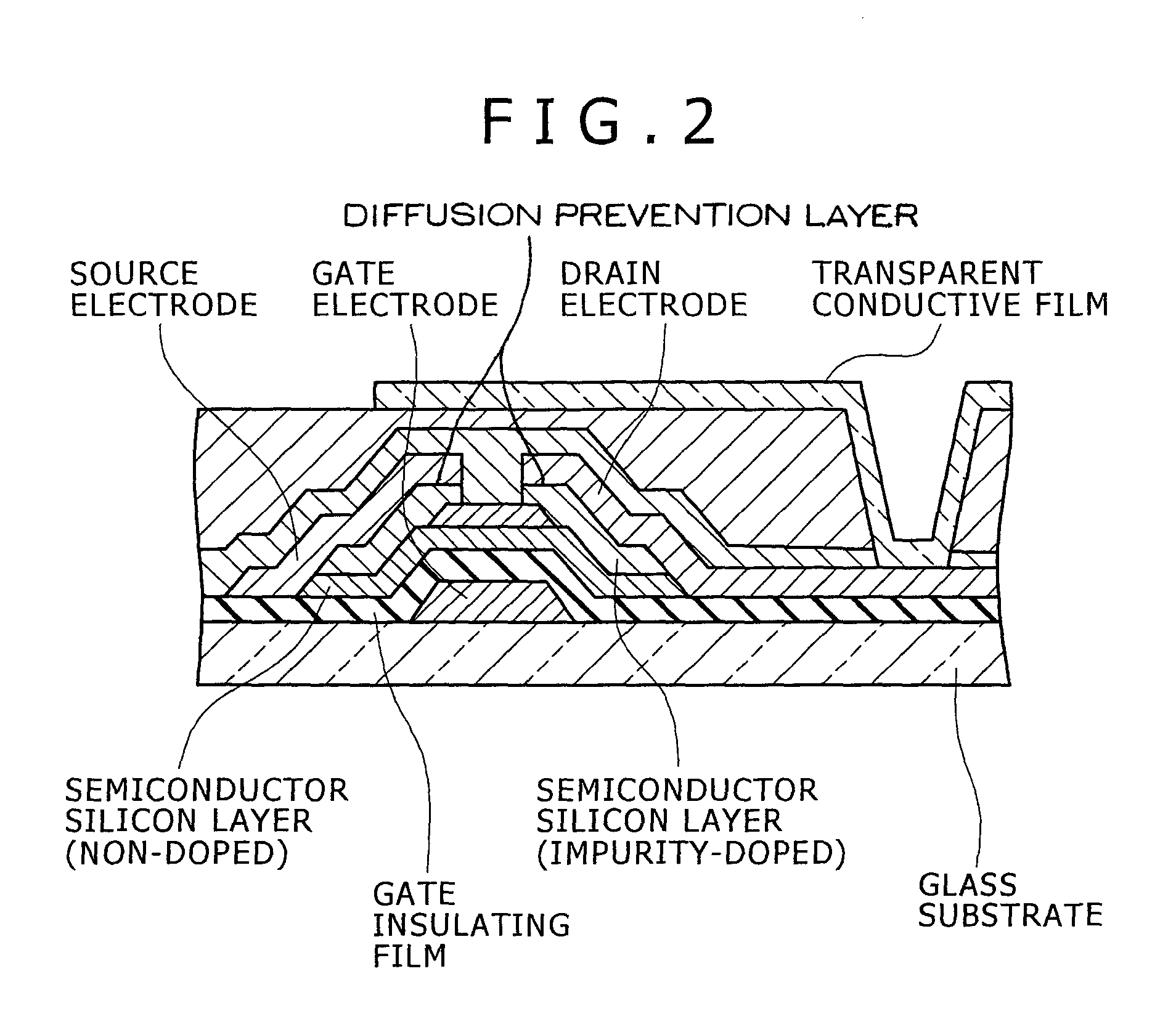
Thin film transistor substrate and display device
a thin film transistor and substrate technology, applied in semiconductor devices, semiconductor/solid-state device details, instruments, etc., can solve the problems of reducing on-current, increasing leak current, and significantly deteriorating semiconductor silicon semiconductor performance, so as to prevent a bad effect on the tft element
- Summary
- Abstract
- Description
- Claims
- Application Information
AI Technical Summary
Benefits of technology
Problems solved by technology
Method used
Image

Examples
examples
[0038]Hereinafter, examples of the invention and a comparative example are described. The invention is not limited to the examples, and can be carried out with being appropriately altered and modified within a scope suitable for the purport of the invention, and all of such alterations and modifications are included in a technical scope of the invention.
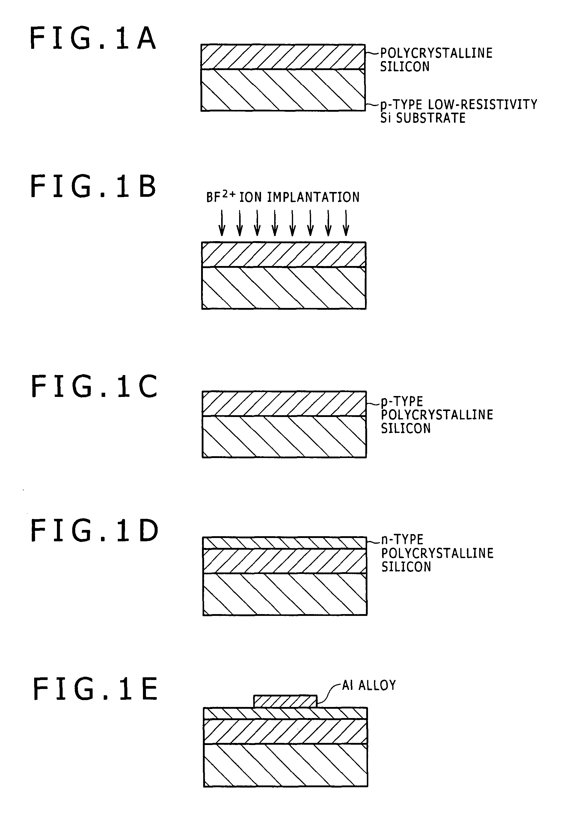
[0039]Evaluation elements (pn-junction elements) according to the examples of the invention and the comparative example were prepared. A process flow is shown in FIGS. 1A to 1E. A preparation method is described below.
[0040]As shown in FIG. 1, first, a polycrystalline silicon film 200 nm in thickness was formed on a p-type low-resistivity silicon substrate by an LPCVD method (FIG. 1A). At that time, SiH4 was used for a source gas. Then, the film was subjected to ion implantation of BF2+ ions at a condition of 10 keV and 3×10¹⁵ / cm2 (FIG. 1B). Then, such an ion-implanted film was subjected to annealing at 800° C. for 30 min to be forme...
example 2
[0045]An Al alloy film 300 nm in thickness was deposited on a glass substrate by the sputtering method. Then, a resist pattern was formed by photolithography, and then the Al alloy film was etched with the resist as a mask to be formed into a stripe pattern shape 100 μm in width and 10 mm in length. A composition of the Al alloy film is the same as that shown in the column of source / drain electrode of Table 1.
[0046]The etched Al alloy film was subjected to annealing at a temperature of 250 to 400° C. for 30 min. Then, the annealed Al alloy film was measured in electrical resistivity by the four-terminal method. A result is shown in a column of electrical resistivity of Table 1. Electrical resistivity of 1.3 times of electrical resistivity of a pure Al film (3.3 μΩ·cm) was used as a standard (3.3*1.3=4.3 μΩ·cm). Compared with the standard, small electrical resistivity was defined to be good, and large electrical resistivity was defined to be bad.
Evaluation of Results in Examples 1 to...
example 3
[0052]Contact performance (contact resistance) when the Al alloy electrode and the transparent conductive film were directly connected to each other was investigated. Samples in which an ITO film was formed on various Al alloy electrodes as shown in Table 2 were formed at a condition of pressure of 3 mTorr and temperature of 200° C. under an Ar gas atmosphere. As the ITO film, a film of ITO including indium oxide added with tin oxide of 10 mass percent was used.
[0053]A Kelvin pattern having a contact hole in 10 μm square was prepared, and contact resistivity was measured by the four-terminal method using the Kelvin pattern. Contact resistivity of 2*10−4 Ωcm2 between a Cr thin film and ITO was used as a standard value, and resistivity not more than the standard value was defined to be good (◯), and resistivity more than the standard value was defined to be bad (x). An evaluation result is shown in Table 2.
[0054]When the Al alloy electrode includes Al—Si alloy, contact resistivity is ...
PUM
 Abstract
Description
Claims
Application Information