Wiring substrate and semiconductor device and method of manufacturing the same

a technology of wiring substrate and semiconductor chip, which is applied in the direction of printed circuit, printed circuit stress/warp reduction, dielectric characteristics, etc., can solve the problems of inability to obtain reliability of connection in the semiconductor chip, deterioration of the operating etc., to prevent deterioration of the performance of the semiconductor chip, good yield, and manufacturing stably

Active Publication Date: 2011-02-22
SHINKO ELECTRIC IND CO LTD
View PDF4 Cites 19 Cited by
  • Summary
  • Abstract
  • Description
  • Claims
  • Application Information

AI Technical Summary

Benefits of technology

[0014]It is an object of the present invention to provide a wiring substrate capable of ensuring sufficient reliability by preventing deterioration in performance of a semiconductor chip even when a high-performance semiconductor chip is flip-chip mounted, and a semiconductor device using this wiring substrate and a method of manufacturing the same.
[0018]In the present invention, the pad wiring portions including the connection pads to which the semiconductor chip is connected are constructed as the aerial wirings that do not contact the underlying layer. Therefore, the connection portions between the semiconductor chip and the connection pads are provided as the flexible structure that moves vertically like a spring. As a result, a thermal stress caused in the semiconductor chip can be relaxed, and reliability of the electrical connection can be improved.
[0019]Also, a stress applied to the semiconductor chip can be absorbed because the connection pads are moved. Therefore, even when the high-performance semiconductor chip that is weak against the stress is mounted, the semiconductor chip can be protected from the stress and deterioration in performance can be prevented.
[0024]In this mode, the semiconductor chip is mounted in a state that the connection pads are fixed on the sacrifice layer, and then the hollow portion is obtained by removing the sacrifice layer. Therefore, the above semiconductor device in which the semiconductor chip is flip-chip connected to the connection pads acting as the moving portion can be manufactured stably with good yield. Otherwise, the hollow portion may be provided before the semiconductor chip is mounted, and then the semiconductor chip may be flip-chip connected to the connection pads that are arranged on the hollow portion.
[0025]As described above, in the present invention, even when the high-performance semiconductor chip is mounted, deterioration of performance of the semiconductor chip can be prevented and thus sufficient reliability can be ensured.

Problems solved by technology

Thus, in some cases the operating performance of the semiconductor chip is deteriorated and also reliability of connection in the semiconductor chip cannot be obtained.

Method used


Image

  • Wiring substrate and semiconductor device and method of manufacturing the same
  • Wiring substrate and semiconductor device and method of manufacturing the same
  • Wiring substrate and semiconductor device and method of manufacturing the same

Examples


first embodiment

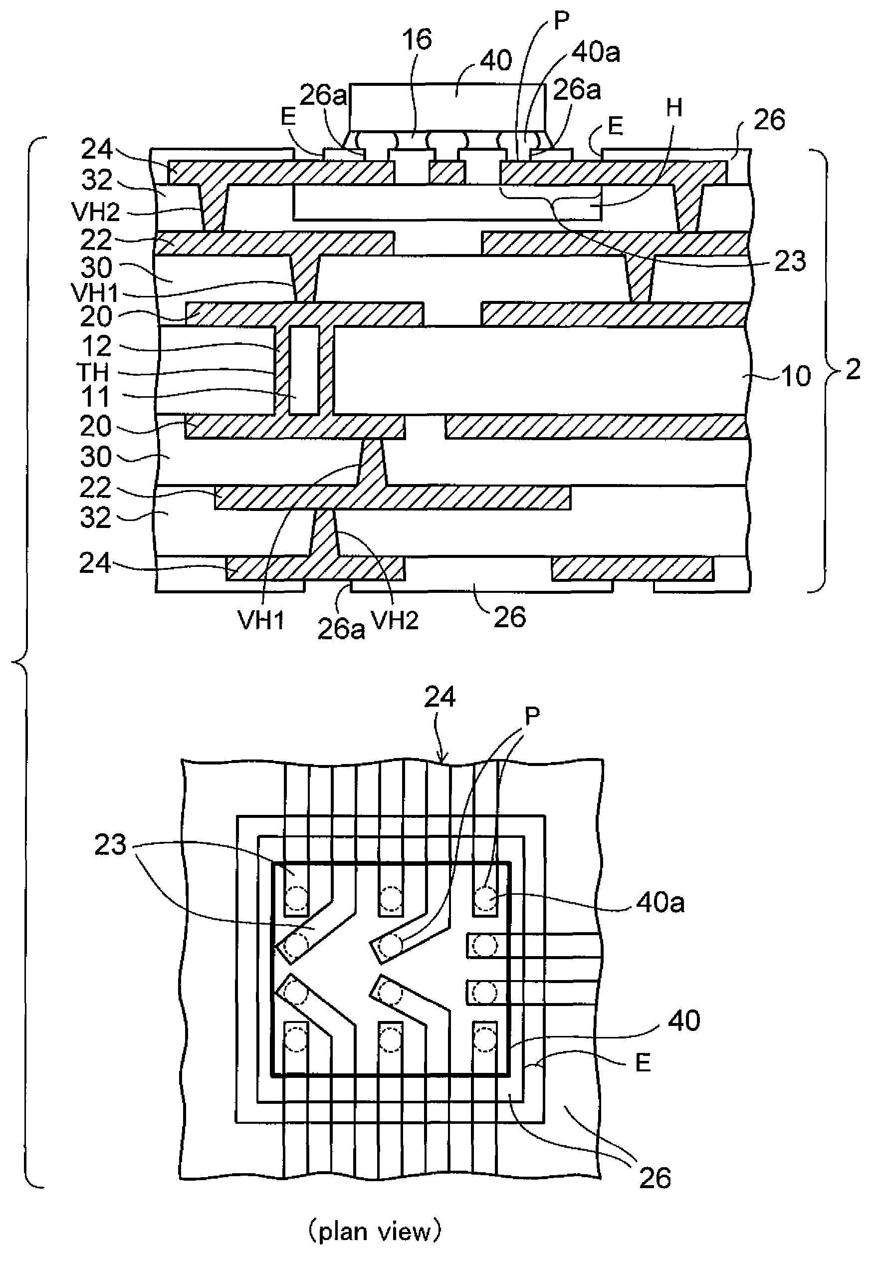
[0040]FIG. 2 to FIG. 8 are views showing a method of manufacturing a semiconductor device according to a first embodiment of the present invention, and FIG. 9 is a view showing the semiconductor device similarly.

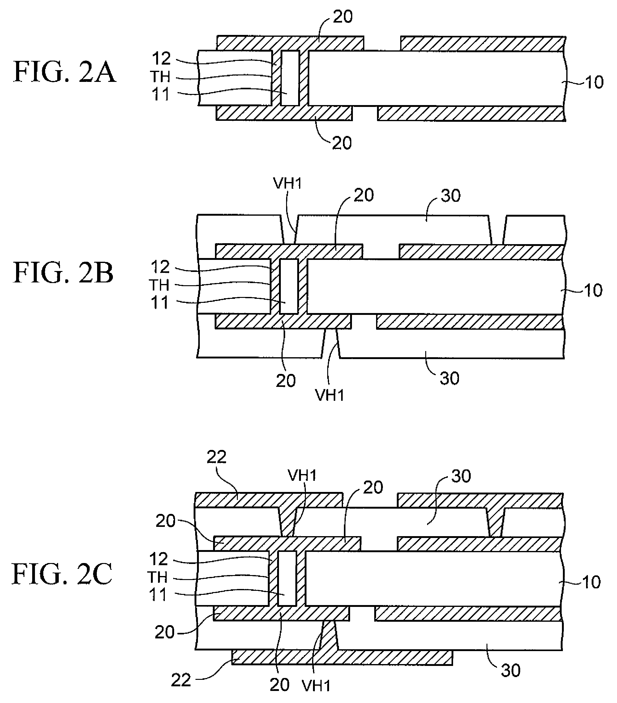
[0041]In the method of manufacturing the semiconductor device of the present embodiment, first, a structure having a sectional structure shown in FIG. 2A is prepared. Through holes TH are provided in a core substrate 10 to pass through it in a thickness direction, and a through hole plating layer 12 is formed on inner surfaces of the through holes TH. A resin 11 is filled in holes in the through holes TH.

[0042]First wiring layers 20 are formed on both surface sides of the core substrate 10 respectively such that both layers are connected mutually via the through hole plating layer 12. As the core substrate 10, a substrate made of a glass cloth that is impregnated with a resin, or the like, a silicon substrate, a glass substrate, or the like is preferably used. When the silic...

second embodiment

[0083]FIG. 13 is a sectional view and a plan view showing a semiconductor device according to a second embodiment of the present invention.

[0084]In the above first embodiment, the connection pads P of the third wiring layers 24 are arranged on the peripheral side of the hollow portion H in a peripheral type. In the second embodiment, as shown in FIG. 13, the connection pads P of the third wiring layers 24 are arranged on the hollow portion H in an area-array type.

[0085]That is, the pad wiring portions 23 of a plurality of third wiring layers 24 are extended to not only the peripheral portion of the hollow portion H but also the center portion, and the connection pads P are arranged on the hollow portion H in grid-like fashion. Accordingly, like the first embodiment, the pad wiring portions 23 are formed as the aerial wiring that is arranged on the hollow portion H and moved vertically respectively.

[0086]Also, the bumps 40a of the semiconductor chip 40 are arranged in an area-array t...


PUM


Abstract

In a wiring substrate of a semiconductor device, a hollow portion is provided under a pad wiring portion including a connection pad, and thus a wiring layer has a cantilever structure in which the pad wiring portion is formed as an aerial wiring, and a semiconductor chip is flip-chip connected to the connection pad. The pad wiring portion including the connection pad is formed on a sacrifice layer which is filled in a recess portion in an interlayer insulating layer of the wiring substrate, then the semiconductor chip is flip-chip connected to the connection pad, and then the hollow portion is provided by removing the sacrifice layer.

Description

CROSS-REFERENCE TO RELATED APPLICATIONS[0001]This application is based on and claims priority of Japanese Patent Application No. 2007-288890 filed on Nov. 6, 2007, the entire contents of which are incorporated herein by reference.BACKGROUND OF THE INVENTION[0002]1. Field of the Invention[0003]The present invention relates to a wiring substrate and a semiconductor device and a method of manufacturing the same and, more particularly, a wiring substrate on which a semiconductor chip is flip-chip mounted, and a semiconductor device constructed by flip-chip mounting the semiconductor chip on the wiring substrate and a method of manufacturing the same.[0004]2. Description of the Related Art[0005]In the prior art, there is a semiconductor device that is constructed by flip-chip mounting a semiconductor on a wiring substrate. As shown in FIG. 1, in a wiring substrate 100 of a semiconductor device in the prior art, through holes TH are provided on a core substrate 200 to pass through there, ...

Claims


Application Information

Patent Timeline
Patent Type & Authority Patents(United States)
IPC IPC(8): H01L21/00H01L21/44H01L23/02
CPCH05K1/0271H01L21/4846H01L23/49811H01L23/49822H01L2924/16152H01L2924/12042H01L2924/10253H01L2924/01019H01L2924/01079H01L2924/01078H05K1/111H05K3/4092H05K3/4644H05K2201/0133H05K2201/0187H05K2201/0397H05K2201/09036H05K2201/10674H01L23/42H01L24/16H01L2224/16225H01L2224/73253H01L2924/01057H01L2924/00
Inventor SUNOHARA, MASAHIROMACHIDA, YOSHIHIRO
Owner SHINKO ELECTRIC IND CO LTD
Why Eureka
Try Eureka