

Touchscreen with carbon nanotube conductive layers
a carbon nanotube and conductive layer technology, applied in the field of touchscreens, can solve the problems of low flexibility of such electrodes, limit the range of potential applications, and high cost of fabrication methods
- Summary
- Abstract
- Description
- Claims
- Application Information
AI Technical Summary
Problems solved by technology
Method used
Image

Examples
invention example 1
Instant Invention Example 1
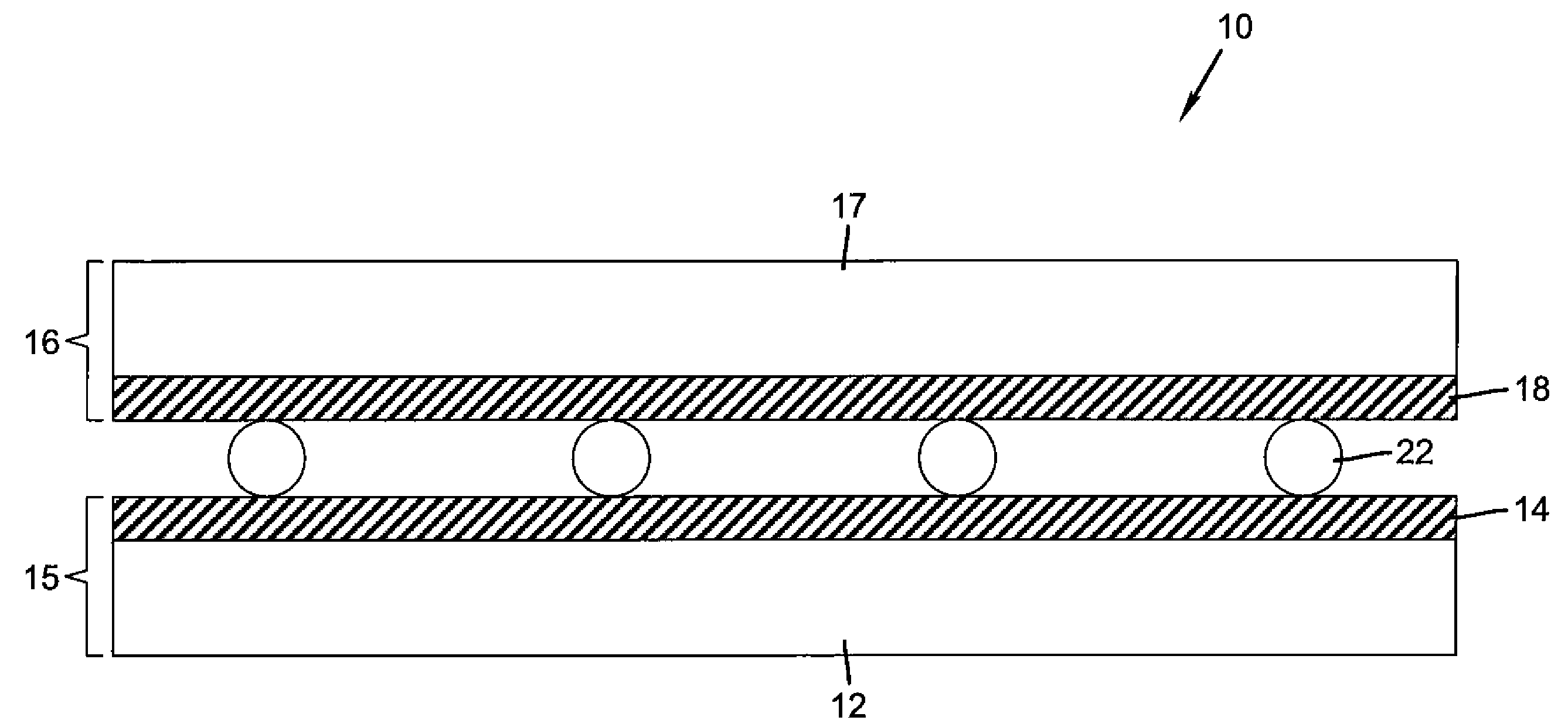
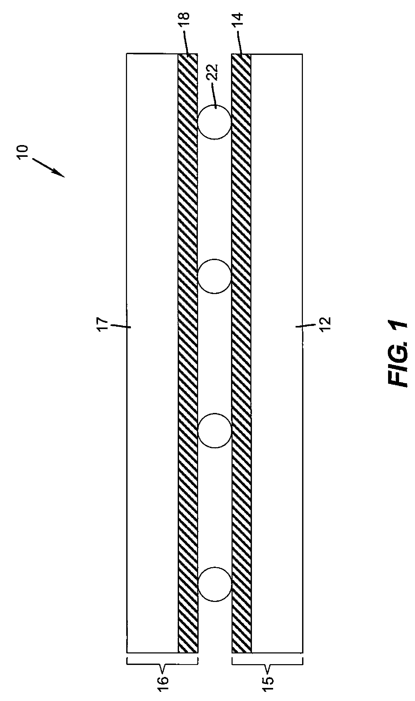
Symmetric Electrode Touch Switch with Single Wall Carbon Nanotubes
[0128]A touchscreen was constructed using Coating C from Table I as electrodes (SWCNT at 32.3 mg / m2). The single point actuation testing was performed and gave the results indicated in FIGS. 11 and 12 below. This symmetric electrode touchscreen demonstrated little change in the force to actuate after completing 1.1 Million SPA without failure, as compared to the comparative examples that all exhibit significant increases in the force to actuate as the number of SPA cycles increased prior to failure. The on-state resistance of instant invention example 1 shows essentially no deviation after 1.1 Million SPA. This symmetric electrode touchscreen demonstrates the significant robustness and operability conferred by using the instant invention.
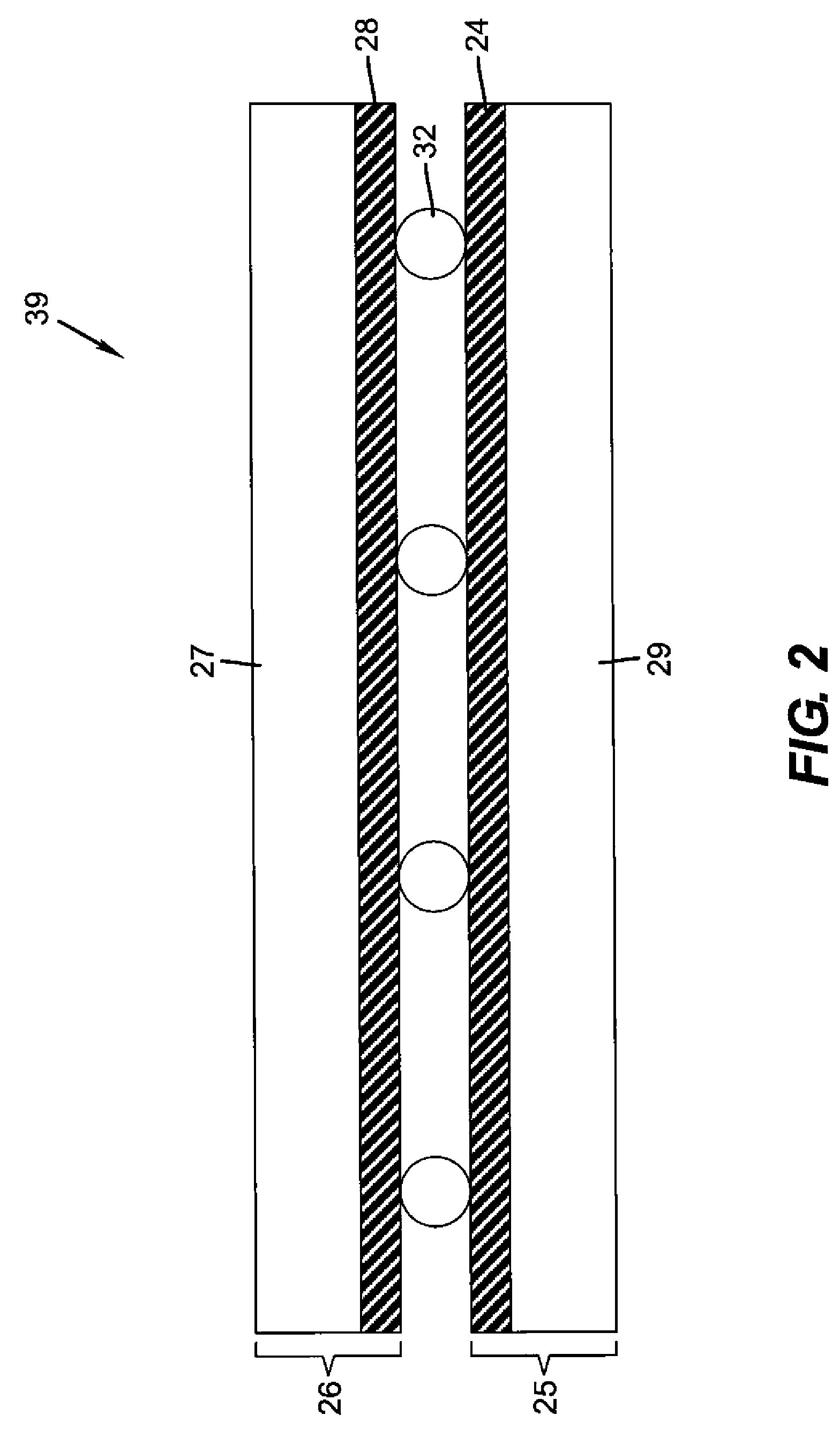
Instant Invention 2
Symmetric Electrode Touch Switch with Single Wall Carbon Nanotubes
[0129]A touchscreen was constructed using Coating D from Table I (SWCNT...
PUM
| Property | Measurement | Unit |
|---|---|---|
| outer diameter | aaaaa | aaaaa |
| outer diameter | aaaaa | aaaaa |
| diameter | aaaaa | aaaaa |
Abstract
Description
Claims
Application Information