

Thin film transistor array substrate and fabricating method thereof
a thin film transistor and array substrate technology, applied in the direction of basic electric elements, semiconductor devices, electrical equipment, etc., can solve the problems of increased manufacturing cost, power consumption, signal distortion, etc., to reduce the manufacturing cost, simplify the manufacturing process, and reduce the mask process
- Summary
- Abstract
- Description
- Claims
- Application Information
AI Technical Summary
Benefits of technology
Problems solved by technology
Method used
Image

Examples
first embodiment
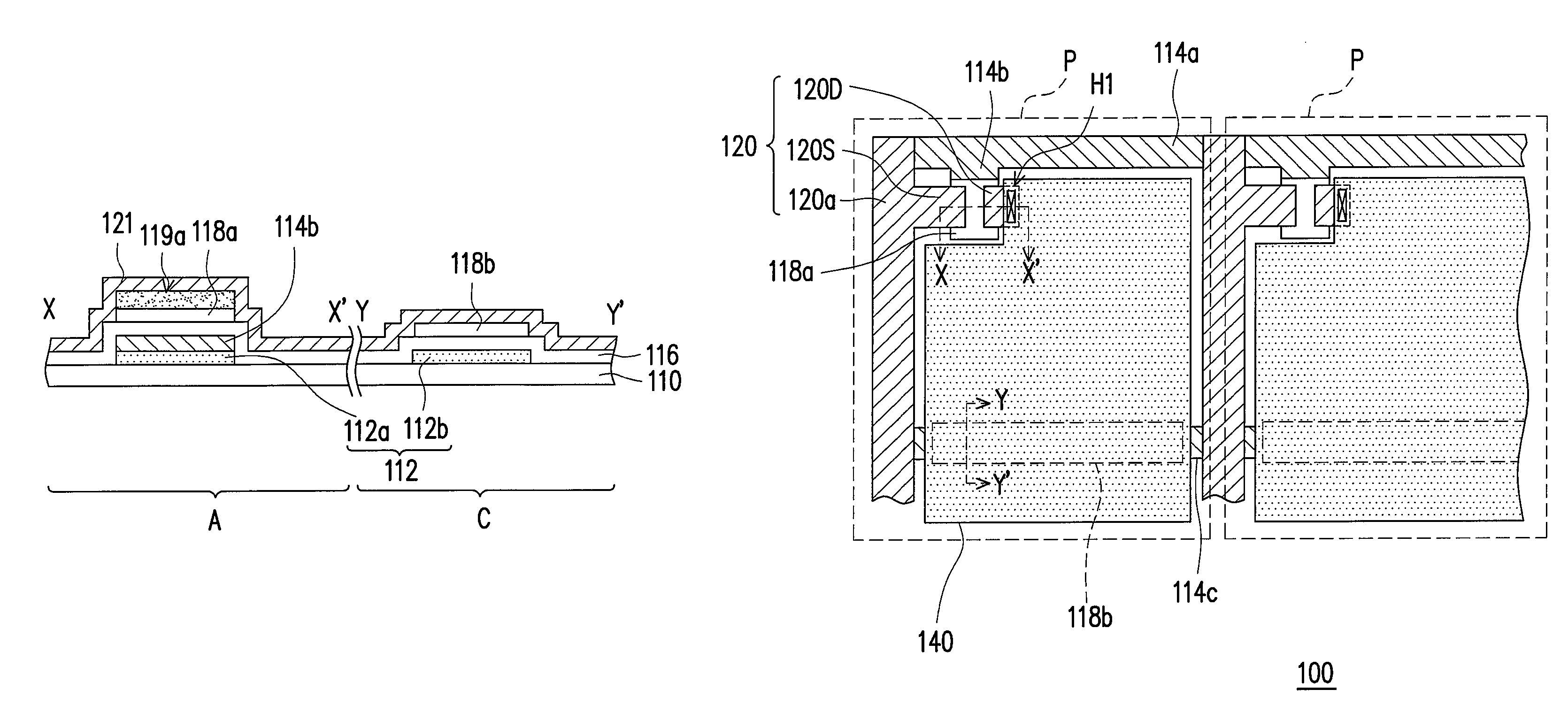
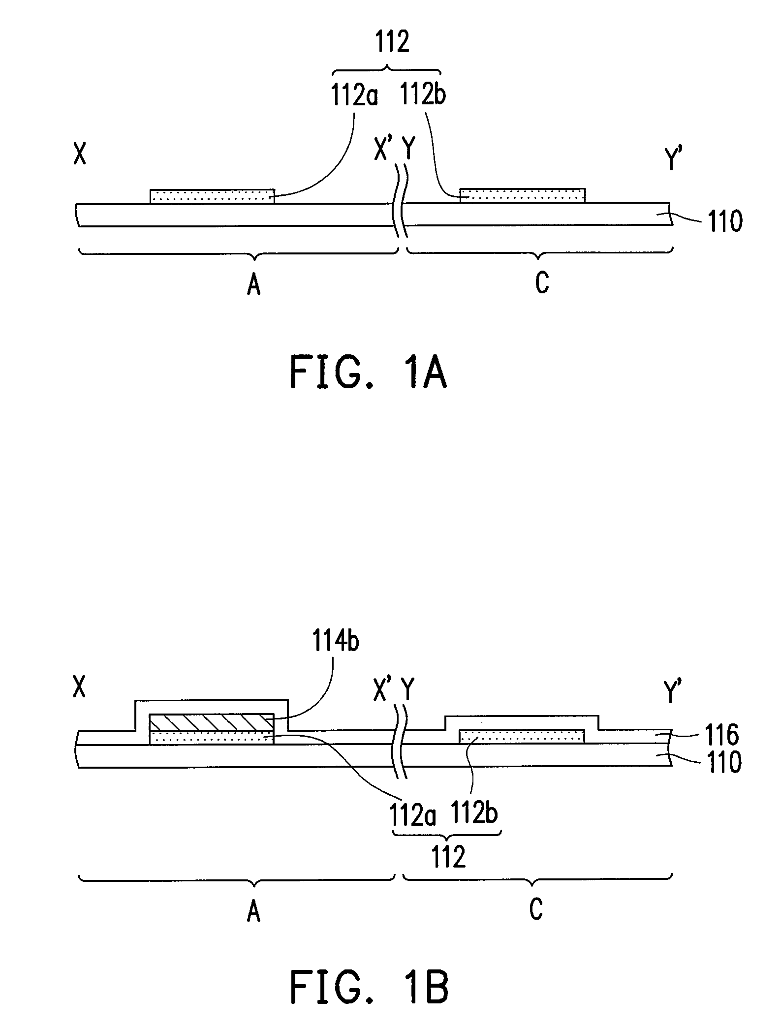
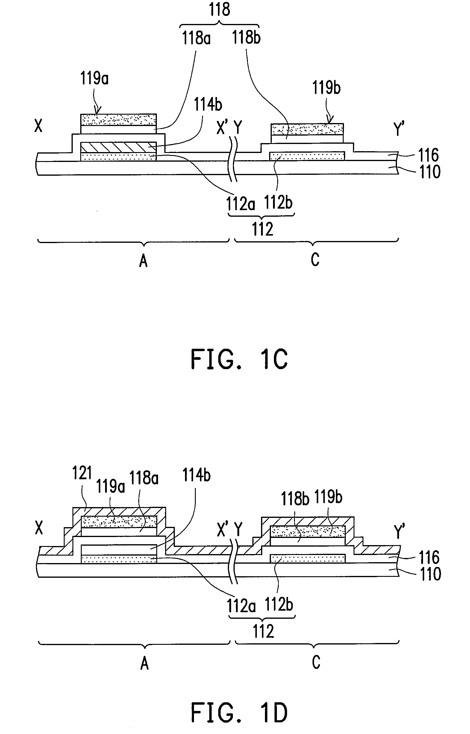
[0039]FIGS. 1A˜1H are cross-sectional views illustrating the fabricating flow of a thin film transistor (TFT) array substrate according to a first embodiment of the present invention, and FIGS. 2A˜2E are top views illustrating the fabricating flow of the TFT array substrate according to the first embodiment of the present invention. Referring to FIG. 1A and FIG. 2A, first, a substrate 110 is provided, and the substrate 110 has a plurality of pixel preset regions P arranged as an array (only two pixel preset regions P are illustrated demonstratively in FIG. 2A), and each pixel preset region P has an active device region A and a capacitor region C. A patterned transparent conductive layer 112 is then formed on the substrate 110 to form a first transparent conductive pattern 112a in each active device region A and a second transparent conductive pattern 112b in each capacitor region C.
[0040]To be specific, the transparent conductive layer 112 may be formed by depositing a transparent c...
second embodiment
[0053]FIGS. 3A˜3H are cross-sectional views illustrating the fabricating flow of a TFT array substrate according to a second embodiment of the present invention, and FIGS. 4A˜4F are top views illustrating the fabricating flow of the TFT array substrate according to the second embodiment of the present invention. Referring to FIG. 3A and FIG. 4A, a substrate 110 is first provided and the substrate 110 has a plurality of pixel preset regions P arranged as an array (only two pixel preset regions P are illustrated demonstratively in FIG. 4A). Each of the pixel preset regions P has an active device region A and a capacitor region C. A patterned transparent conductive layer 112 is then formed on the substrate 110 to form a first transparent conductive pattern 112a in each active device region A and a second transparent conductive pattern 112b in each capacitor region C. It should be noted here that the second transparent conductive patterns 112b in adjacent pixel preset regions P are conn...
PUM
 Abstract
Description
Claims
Application Information