Bowed wafer hybridization compensation

a hybridization compensation and wafer technology, applied in the field of wafer processing, can solve the problems of not uniformly flat across the wafer area and unsuitability for use of wafers

Active Publication Date: 2010-09-28
CUFER ASSET LTD LLC
View PDF43 Cites 106 Cited by
  • Summary
  • Abstract
  • Description
  • Claims
  • Application Information

AI Technical Summary

Benefits of technology

[0008]Through use of the approaches described herein, bowed wafers can be used with various techniques that allow for via densities, pitch and placement and involve forming small, deep vias in, and electrical contacts for, the wafers—on a chip, die or wafer scale, even though the heights or densities of the contacts thereon are small relative to wafer bow.

Problems solved by technology

However, they are not necessarily uniformly flat across the extent of the wafer.
However, such variations can render a wafer unsuitable for use where the pitch and / or height of the individual contacts is less than or equal to 25 μm, unless further expensive polishing operations are performed to reduce the bow to an acceptable level, if it is possible to do so at all.

Method used


Image

  • Bowed wafer hybridization compensation
  • Bowed wafer hybridization compensation
  • Bowed wafer hybridization compensation

Examples


Embodiment Construction

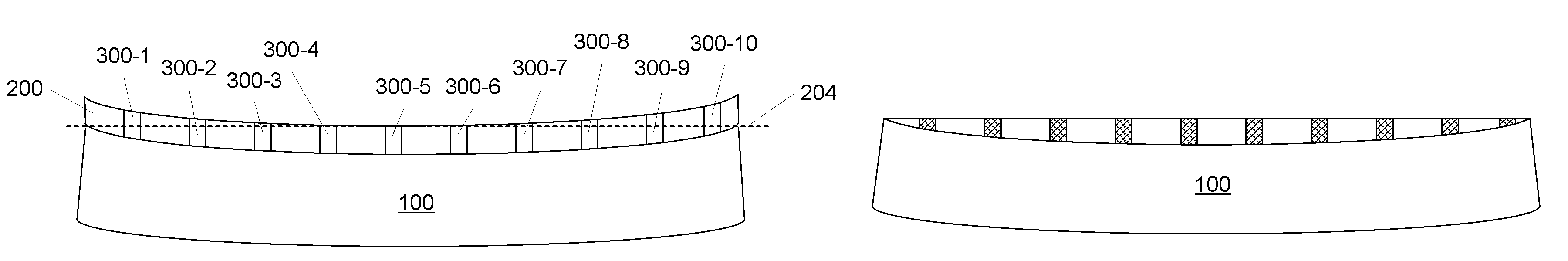
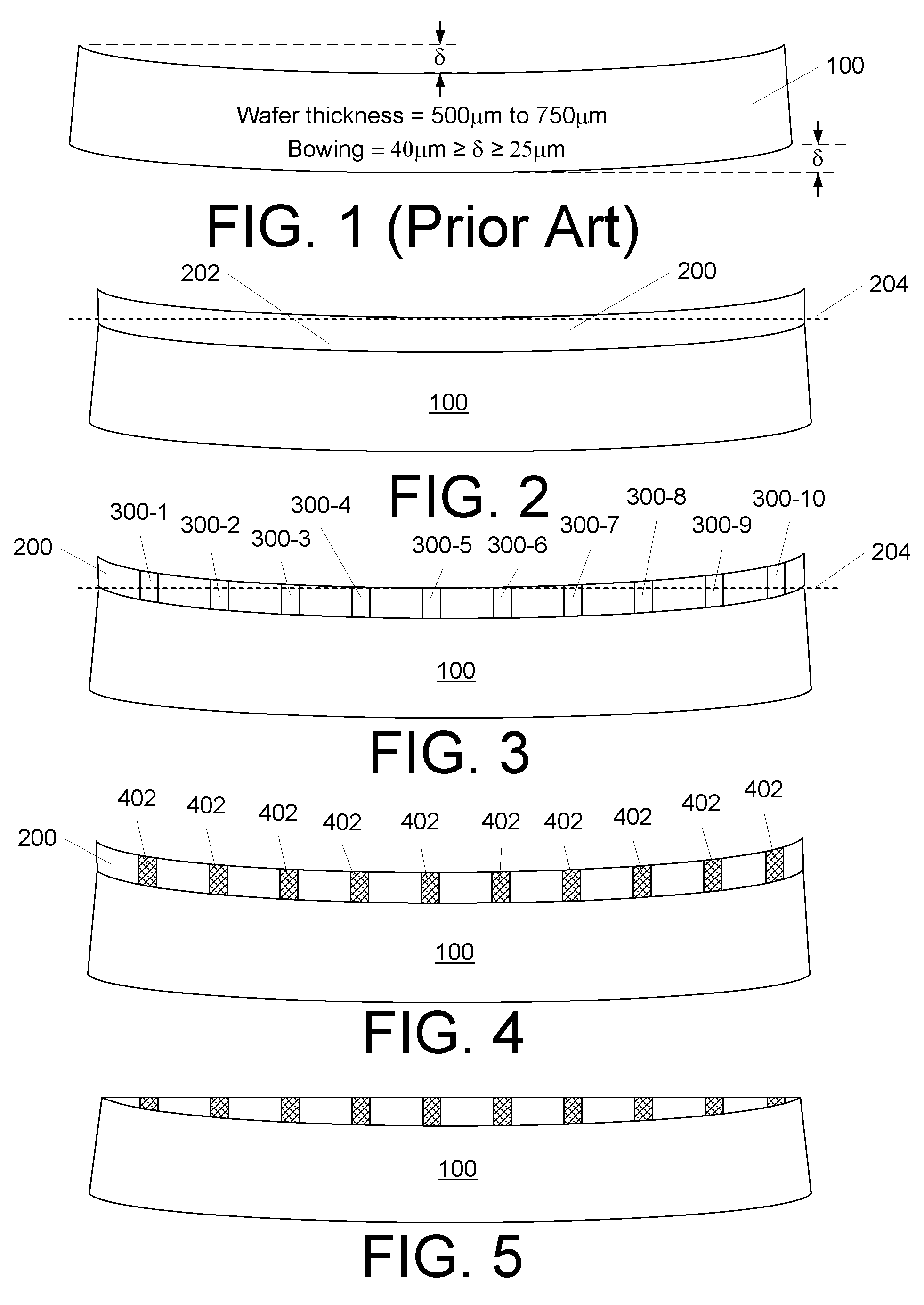
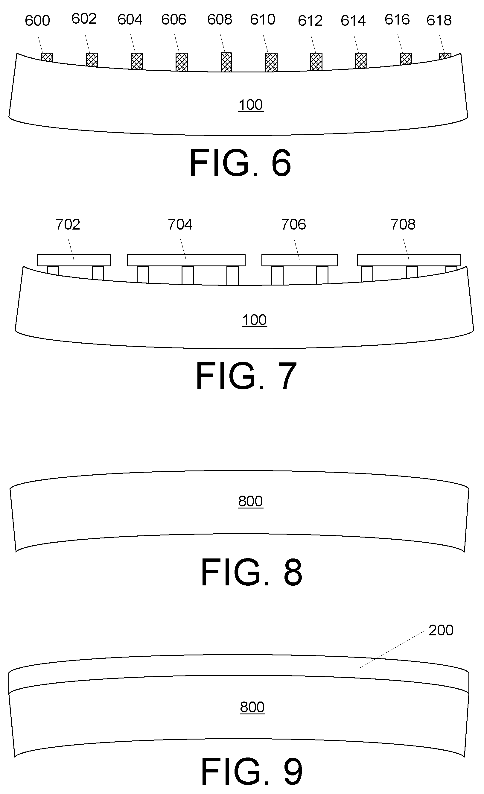
[0018]U.S. patent applications, Ser. Nos. 11 / 329,481, 11 / 329,506, 11 / 329,539, 11 / 329,540, 11 / 329,556, 11 / 329,557, 11 / 329,558, 11 / 329,574, 11 / 329,575, 11 / 329,576, 11 / 329,873, 11 / 329,874, 11 / 329,875, 11 / 329,883, 11 / 329,885, 11 / 329,886, 11 / 329,887, 11 / 329,952, 11 / 329,953, 11 / 329,955, 11 / 330,011 and 11 / 422,551, incorporated herein by reference, describe various techniques for forming small, deep vias in, and electrical contacts for, semiconductor wafers. The techniques allow for via densities, pitch and placement that was previously unachievable and can be performed on a chip, die or wafer scale. In some cases, it is desirable to perform the techniques described therein on a wafer but the contact heights or densities are small relative to wafer bow. Advantageously, we have developed a way to do so. FIGS. 2 through 6 illustrate, in simplified from, use of our approach on a bowed wafer 100 that is considered “dished.” The process is as follows:

[0019]First, as shown in FIG. 2, a material 2...


PUM


Abstract

A planarizing method performed on a non-planar wafer involves forming electrically conductive posts extending through a removable material, each of the posts having a length such that a top of each post is located above a plane defining a point of maximum deviation for the wafer, concurrently smoothing the material and posts so as to form a substantially planar surface, and removing the material. An apparatus includes a non planar wafer having contacts thereon, the wafer having a deviation from planar by an amount that is greater than a height of at least one contact on the wafer, and a set of electrically conductive posts extending away from a surface of the wafer, the posts each having a distal end, the distal ends of the posts collectively defining a substantially flat plane.

Description

FIELD OF THE INVENTION[0001]The present invention relates to wafer processing and, more particularly, to wafer processing for electrical connections.BACKGROUND[0002]Semiconductor wafers are typically highly polished with very smooth surfaces (i.e. deviations of less than 1 nm). However, they are not necessarily uniformly flat across the extent of the wafer. The same is true for wafers of ceramic or other materials. Flatness variation, called “wafer bow,” may be a result of the wafer manufacturing process itself or processing of the wafer (e.g. through depositing of metal or dielectric onto the wafer) and can be on the order of 25 μm or more on the concave and / or convex side. If the polished side is concave, the wafer is often referred to as “dished” whereas if it is convex the wafer is called “bowed.” Note however, that an individual wafer can concurrently have both types of non-planarities (i.e. one portion is bowed whereas another portion is dished.[0003]For simplicity herein, the...

Claims


Application Information

Patent Timeline
Patent Type & Authority Patents(United States)
IPC IPC(8): H01L21/76H01L21/311H01L21/44H01L21/31
CPCH01L24/12H01L24/11H01L21/461H01L2224/1703H01L24/81H01L2224/1147H01L2224/13099H01L2224/81193H01L2224/81801H01L2924/01027H01L2924/01029H01L2924/01033H01L2924/01046H01L2924/01047H01L2924/01078H01L2924/3511H01L2924/15787H01L2924/00014H01L2924/00011H01L2924/00H01L2224/0401H01L21/304
Inventor TREZZA, JOHN
Owner CUFER ASSET LTD LLC
Why Eureka
Try Eureka