

Film forming method, fabrication process of semiconductor device, computer-readable recording medium and sputtering apparatus
a technology of film forming and semiconductor devices, which is applied in the direction of vacuum evaporation coating, transistors, coatings, etc., can solve the problems of damage to the semiconductor devices formed thereon, and achieve the effect of facilitating plasma ignition and simple construction
- Summary
- Abstract
- Description
- Claims
- Application Information
AI Technical Summary
Benefits of technology
Problems solved by technology
Method used
Image

Examples
first embodiment
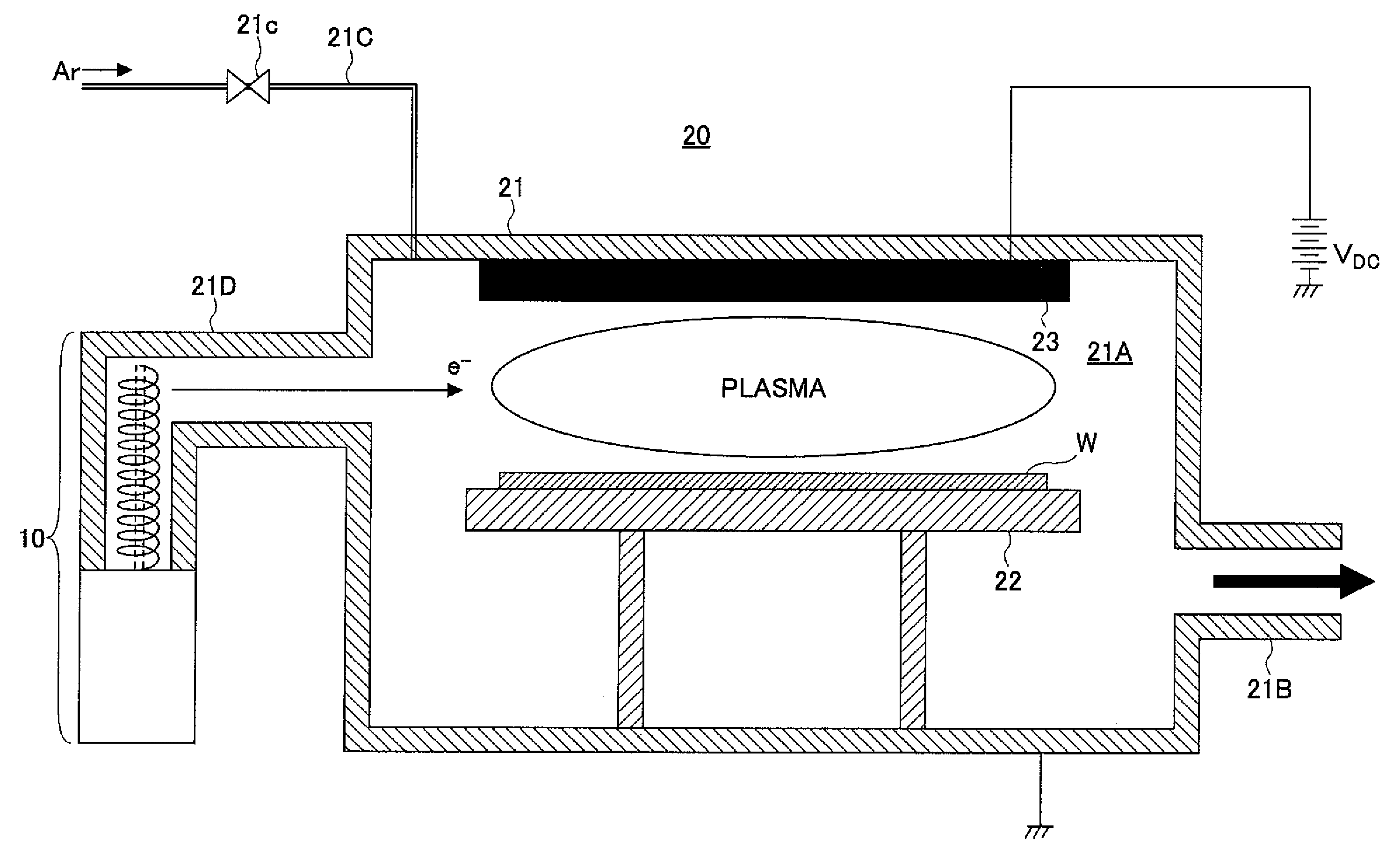
[0068]FIG. 3 is a diagram showing the construction of a sputtering apparatus 20 used with a first embodiment of the present invention.
[0069]Referring to FIG. 3, the sputtering apparatus 20 includes a processing vessel 21 defining therein a processing space 21A in which plasma is formed for the sputtering processing, wherein the processing vessel 21 accommodates therein a stage 22 holding a substrate W to be processed thereon.
[0070]The processing space 21A is evacuated via an evacuation port 21B provided to the processing vessel 21 and is supplied with a rare gas such as Ar, Kr, Ne, Xe, He, or the like, from a gas line 21C via a valve 21c.
[0071]Further, a sputter target 23 of a metal such as Co, Ni, or the like, is held in the processing vessel 21 so as to face the substrate W on the stage 22, wherein a high positive voltage in the range of 300-1000V is applied to the sputter target 23 by a DC power supply VDC.
[0072]Thus, upon formation of plasma in the processing space 21A by the e...
second embodiment
[0098]FIG. 7 shows the construction of an ion gauge 10A used with the sputtering apparatus according to a second embodiment of the present invention, wherein those parts corresponding to the parts explained previously are designated by the same reference numerals and the description thereof will be omitted.
[0099]Referring to FIG. 7, the collector 13 is grounded via a switch 13X controlled by the controller 31 with the ion gauge 10A of the present embodiment.
[0100]Thus, with the present embodiment, the switch 13X is closed when re-energizing the ion gauge 10A in the step 4 of FIG. 5, and with this, the protective function of the ion gauge is canceled. At the same time, application of positive voltage to the collector 13 is canceled.
[0101]By using the ion gauge 10A of FIG. 7, there is no possibility of the ion gauge being erroneously shutdown at the time of the plasma ignition operation and there is no longer the need of disposing the ion gauge in the manner hidden from the plasma con...
third embodiment
[0103]FIGS. 9A-9L are diagrams showing the outline of the fabrication process of a semiconductor device 40 according to a third embodiment of the present invention, while FIG. 10 shows the flowchart corresponding to the steps of FIGS. 9H-9L.
[0104]Referring to FIG. 9A, the semiconductor device 40 is an n-channel MOS transistor formed on a silicon substrate 14, wherein the silicon substrate 41 is formed with a device region 41A by a device isolation region 41I of STI (shallow trench isolation) structure. The device region 41A is formed with a p-type well (not shown), for example.
[0105]Next, in the step of FIG. 9B, an SiON film 42 is formed on the silicon substrate 41 with a thickness of 1-2 nm, and a polysilicon film 43 is formed on the SiON film 42 in the step of FIG. 41C typically with a thickness of 100 nm.
[0106]Next, in the step of FIG. 9D, the polysilicon film 43 and the SiON film 42 underneath the polysilicon film 43 are subjected to a patterning process, and there are formed a ...
PUM
| Property | Measurement | Unit |
|---|---|---|
| gate length | aaaaa | aaaaa |
| gate length | aaaaa | aaaaa |
| bias voltage | aaaaa | aaaaa |
Abstract
Description
Claims
Application Information