Method for improving yield of a layout and recording medium having the layout

a technology of layout and recording medium, which is applied in the field of improving the yield of semiconductor integrated circuits, can solve the problems of difficult to obtain satisfactory yield, difficult to apply the rr to a rule having a large difference between the gr value and the rr value, and difficult to integrate patterns into the semiconductor ic. achieve the effect of improving the yield of layou

Inactive Publication Date: 2010-10-19
SAMSUNG ELECTRONICS CO LTD
View PDF6 Cites 11 Cited by
  • Summary
  • Abstract
  • Description
  • Claims
  • Application Information

AI Technical Summary

Benefits of technology

[0014]It is therefore a feature of an embodiment of the present invention to provide a method for improving the yield of a layout by adding a margin to rules associated with a metal pattern, a poly pattern, or an active pattern based on the overall fail rate of the patterns.
[0015]It is therefore another feature of an embodiment of the present invention to provide a recording medium having recorded the method for improving the yield of the layout thereon.
[0016]At least one of the above and other features and advantages of the present invention may be realized by providing a method for improving a yield of a layout, which may include selecting a pattern that does not satisfy at least one of multiple rules of the layout, adding a margin to a predetermined value of the at least one of the rules of the selected pattern, based on a ground rule and a recommended rule of the at least one of the rules, calculating an overall fail rate of at least one of the rules that varies according to the addition of the margin, and determining the adjusted margin to be added based on the calculated overall fail rate.
[0018]At least one of the above and other features and advantages of the present invention may be realized by providing a method for improving a yield of a layout, which may include selecting a pattern that does not satisfy at least one of a plurality of rules within the layout, determining whether the rules associated with the selected pattern have a space to add a margin, determining a range of the margin to be added to the value of at least one rule, ascertaining the types of rules associated with the selected pattern, differentiating the rules into rules having increasing values and rules having decreasing values with the margin is added to a rule that does not satisfy a recommended rule, adding the margin to a predetermined value of the at least one of the plurality of rules associated with selected pattern, based on a ground rule and the recommended rule of each of the plurality of rules, calculating an overall fail rate of at least one of the plurality of rules that varies according to the addition of the margin, and determining an adjusted margin to be added based on the calculated overall fail rate.

Problems solved by technology

With current developments in semiconductor IC layout technology, a design of multiple patterns may be conducted with associated rules having values of sub-microns or less, and thus it may be difficult to obtain a satisfactory yield by only using the GR.
When the values of the rules in the layout having a predetermined size are greater than the values of the RR, it may be difficult to integrate the patterns into the semiconductor IC.
However, the rule associated with the pattern is divided into the GR and the RR, and it may be difficult to apply the RR to a rule having a large difference between the GR value and the RR value because the fixed size of the layout.
In addition, the processor or user may have difficulty in setting a standard for determining the threshold value, and when a percentage of patterns that satisfy the RR is less than the threshold value, the patterns may not be able to be corrected because the space of the layout may be insufficient.

Method used


Image

  • Method for improving yield of a layout and recording medium having the layout
  • Method for improving yield of a layout and recording medium having the layout
  • Method for improving yield of a layout and recording medium having the layout

Examples


Embodiment Construction

[0026]Korean Patent Application No. 10-2006-0078456, filed on Aug. 19, 2006, in the Korean Intellectual Property Office, and entitled: “Method for Improving Yield of Layout and Recording Medium Having the Same,” is incorporated by reference herein in its entirety.

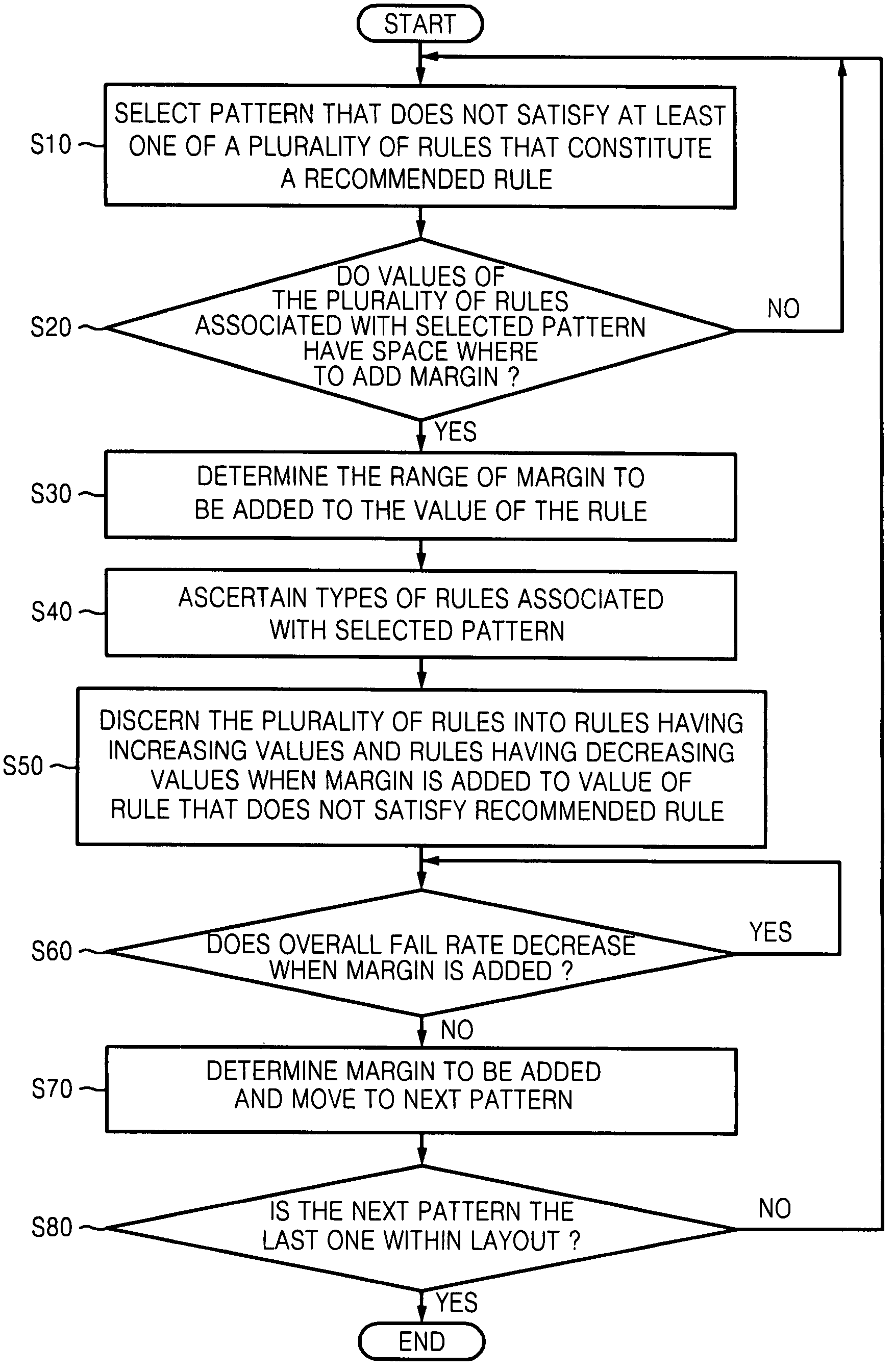
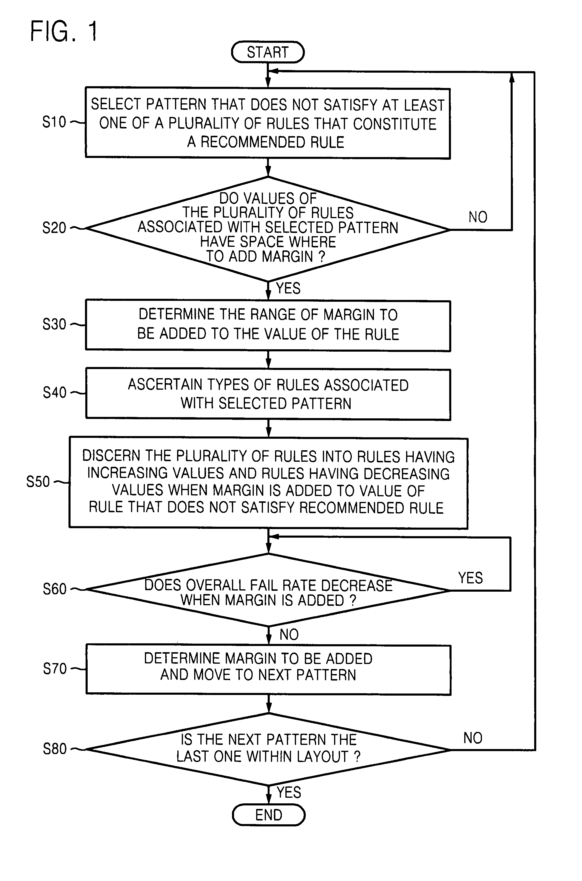
[0027]The present invention will now be described more fully hereinafter with reference to the accompanying drawings, in which exemplary embodiments of the invention are illustrated. The invention may, however, be embodied in different forms and should not be construed as limited to the embodiments set forth herein. Rather, these embodiments are provided so that this disclosure will be thorough and complete, and will fully convey the scope of the invention to those skilled in the art.

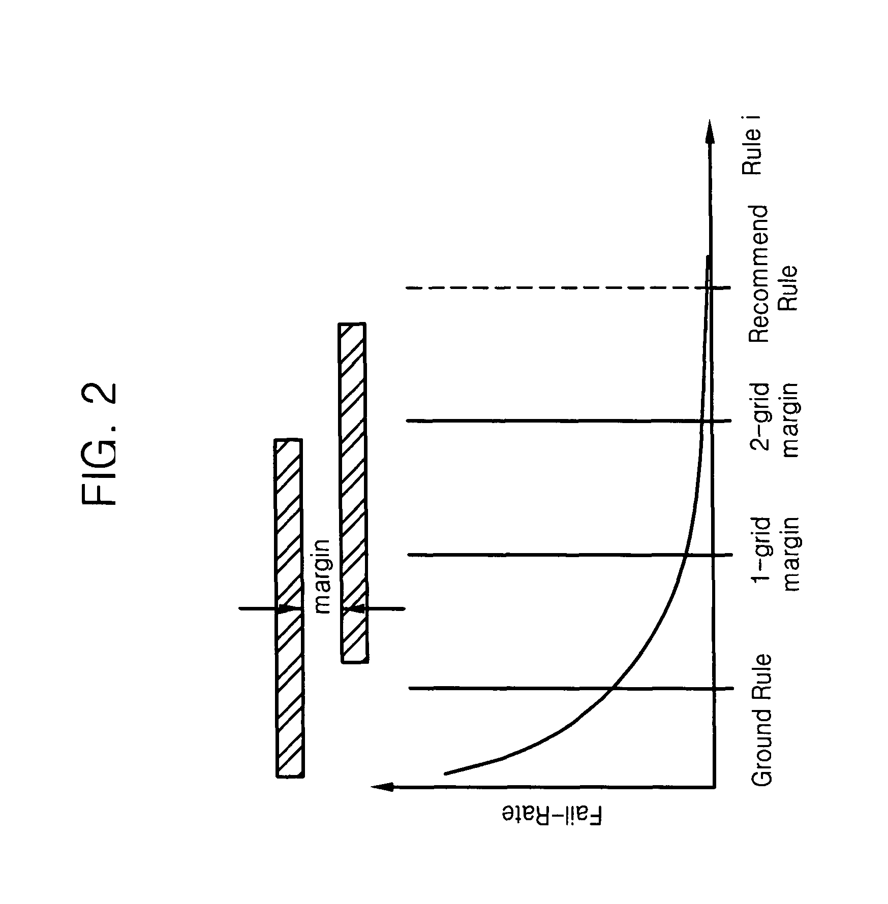
[0028]In the drawing figures, the dimensions of layers and regions may be exaggerated for clarity of illustration. It will also be understood that when a layer or element is referred to as being “on” another layer or substrate, it can be direct...


PUM


Abstract

A yield of a semiconductor layout may be improved by selecting a pattern that does not satisfy at least one of multiple rules within the layout, adding a margin to a predetermined value of the at least one of the rules associated with selected pattern, based on a ground rule and a recommended rule of each of the rules, calculating an overall fail rate of at least one of the rules that varies according to the addition of the margin, and determining an adjusted margin to be added based on the calculated overall fail rate.

Description

BACKGROUND OF THE INVENTION[0001]1. Field of the Invention[0002]The present embodiments relate to a method for improving a yield of semiconductor integrated circuits (ICs). More particularly, the present embodiments relate to a method for improving a yield of a semiconductor IC by adding a margin to a metal pattern, a poly (polysilicon) pattern, or an active pattern of a layout of the semiconductor IC, and a recording medium having the method recorded thereon.[0003]2. Description of the Related Art[0004]A semiconductor layout may be designed based on rules associated with each of multiple patterns. Each of the rules may play an important role in arranging the corresponding pattern within a semiconductor layout.[0005]Each of the rules may be based on a ground rule (GR) measured in a manufacturing part. The GR is also referred to as a minimum rule, and may correspond to a minimum value of each of rules associated with a metal pattern, a poly pattern, and an active pattern.[0006]When a...

Claims


Application Information

Patent Timeline
Patent Type & Authority Patents(United States)
IPC IPC(8): G06F17/50
CPCG06F17/5068G06F30/39G03F1/70G03F7/70433G03F7/70491G03F7/70508
Inventor CHO, DAE HYUNG
Owner SAMSUNG ELECTRONICS CO LTD
Why Eureka
Try Eureka