Touching microlens structure for a pixel sensor and method of fabrication

a microlens and sensor technology, applied in the direction of instruments, photomechanical equipment, diffusion transfer processes, etc., can solve the problems of wasting more light between the lenses, microlens structures formed in this manner exhibit light loss between the lenses, etc., to increase the sensitivity of pixel sensors, eliminate the formation of gap space, effect of increasing sensitivity

Inactive Publication Date: 2010-11-09
TAIWAN SEMICON MFG CO LTD
View PDF22 Cites 0 Cited by
  • Summary
  • Abstract
  • Description
  • Claims
  • Application Information

AI Technical Summary

Benefits of technology

[0010]This invention addresses a structure and method for increasing the sensitivity of pixel sensors (e.g., optical image sensors) by eliminating the gap space formed between adjacent microlens structures in a pixel imaging array. This is achieved by forming a webbed lens that provides advantages as having substantially no gap; however, further the formed microlens structure has a radius of curvature at the 45° degree that is matched to the radius of curvature of the lens cross-section to increase sensitivity for receiving more light. Preferably, the corners are open because they get more light (at the crosses) where two pixels meet; however, the corners are formed down from the webbed edges—so the 45° degree radius of curvature can be matched to the cross-section maximizing the light collection.
[0011]Thus, according to a first aspect of the invention, there is provided a touching microlens structure whereby the gaps between adjacent microlens structures is tailored to achieve a level of horizontal webbing and corner openness such that all light incident to the microlens is optimally captured and focused into the pixel active device area. Thus, the microlens array for the pixel sensor comprises microlens structures that remain connected and perfectly formed, i.e., the 45° degree radius of curvature of the formed lens structure is matched to the cross-section of the formed lens structure thereby maximizing the light collection, even at the reduced pixel sizes.
[0012]According to a second aspect of the invention, there is provided a method for fabricating a touching microlens structure for a pixel array or sensor whereby the gaps between adjacent microlens structures is tailored to achieve a level of horizontal webbing and corner openness such that all light incident to the microlens is optimally captured and focused into the pixel active device area. In accordance with this aspect of the invention, a solution is provided whereby the lithographic image in sub-resolution remains connected with a partial opening and when this image is flowed to form a lens, the lenses remain connected and perfectly formed. In addition, it is found that by further underexposing out this image, thin lenses can be made with thick material. Thus, instead of controlling the microlens thickness with resist thickness—which becomes difficult as the lens get thinner as they scale, the thickness is adjusted by the lithographic conditions (sub-threshold exposure, develop, blanket exposure and post expose bake, or develop). In this manner, a microlens structure is achievable that remains connected and perfectly formed, and beneficially, the 45° degree radius of curvature of the formed lens structure can be matched to the cross-section of the formed lens structure, thereby maximizing the light collection.

Problems solved by technology

It is the case however, that the microlens structures formed in this manner exhibit light loss between the lenses.
It is further the case that the smaller the pixel size, the greater the percentage of light is wasted between the lenses.

Method used


Image

  • Touching microlens structure for a pixel sensor and method of fabrication
  • Touching microlens structure for a pixel sensor and method of fabrication
  • Touching microlens structure for a pixel sensor and method of fabrication

Examples


Embodiment Construction

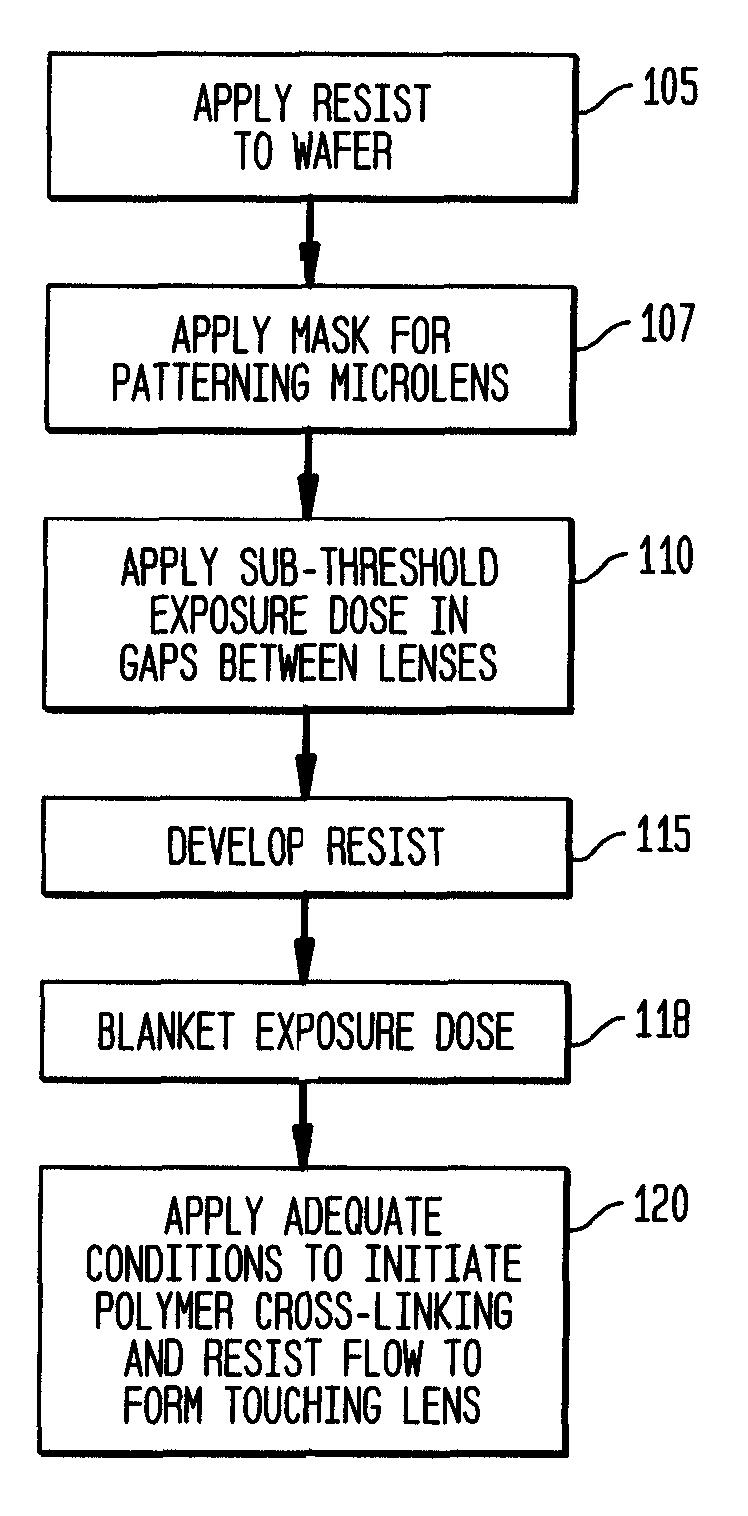
[0022]A method for forming a webbed microlens structure according to the invention includes first flowing a patterned photoresist on providing a smooth planarization layer or equivalent substrate. However, to achieve touching of the microlenses, according to the invention, the photoresist pattern is “webbed” before flow. Webbing is achieved by a variety of methods: for instance, by controlling (e.g., reducing) the initial UV exposure dose; focusing can be set at a non-optimal value; develop time, temperature, or concentration can be reduced; or, the post exposure bake can be used to affect the rate of cross-linking polymers of the resist material. The mask image may additionally be compensated or the wavelength or numerical aperture (NA) / Sigma combination of the lithography tool altered to web the image. After application of one or more of these process modifications, the bottom of the photoresist in the transferred images connects to the bottom of the adjacent gap, i.e. a web is fo...


PUM

PropertyMeasurementUnit
temperatureaaaaaaaaaa
radiusaaaaaaaaaa
radiusaaaaaaaaaa

Abstract

A structure and method for increasing the sensitivity of pixel sensors by eliminating a gap space formed between adjacent microlens structures in a pixel sensor array. Advantageously, exposure and flowing conditions are such that adjacent microlens structures touch (are webbed) at a horizontal cross-section, yet have a round lens shape in all directions. Particularly, exposure and flowing conditions are such that each touching microlens structure is formed to have a matched uniform radius of curvature at a horizontal cross-section and at a 45 degree cross-sections.

Description

BACKGROUND OF THE INVENTION[0001]1. Field of the Invention[0002]The present invention related generally to the fabrication of semiconductor pixel sensor arrays, and more particularly, to a novel semiconductor pixel structure and novel process therefor for increasing the sensitivity of the pixel sensors by optimizing the formed microlens structure.[0003]2. Discussion of the Prior Art[0004]CMOS image sensors are beginning to replace conventional CCD sensors for applications requiring image pick-up such as digital cameras, cellular phones, PDA (personal digital assistant), personal computers, and the like. Advantageously, CMOS image sensors are fabricated by applying present CMOS fabricating process for semiconductor devices such as photodiodes or the like, at low costs. Furthermore, CMOS image sensors can be operated by a single power supply so that the power consumption for that can be restrained lower than that of CCD sensors, and further, CMOS logic circuits and like logic processi...

Claims


Application Information

Patent Timeline
Patent Type & Authority Patents(United States)
IPC IPC(8): H01L31/0232G03F7/20
CPCH01L27/14627H01L27/14685H01L31/0232H01L31/02327
Inventor HOAGUE, TIMOTHY J.LEIDY, ROBERT K.
Owner TAIWAN SEMICON MFG CO LTD
Why Eureka
Try Eureka