Check patentability & draft patents in minutes with Patsnap Eureka AI!

Source/drain stressors formed using in-situ epitaxial growth

a stressor and source technology, applied in the field of source/drain stressors formed using in-situ epitaxial growth, can solve the problems of gate oxide attack on the material used for hf clean can, and lower channel strain,

Active Publication Date: 2010-11-16
NXP USA INC
View PDF6 Cites 9 Cited by
  • Summary
  • Abstract
  • Description
  • Claims
  • Application Information

AI Technical Summary

Benefits of technology

This approach reduces series resistance and maintains high channel strain by forming in-situ doped epitaxial regions with a natural lattice constant different from the semiconductor layer, effectively addressing the limitations of conventional methods.

Problems solved by technology

The materials used for HF clean can, however, attack the gate oxide.
Implanting of dopants into source / drain regions can cause other problems.
The relaxed stressor layers create lower strain in the channel region and thus are not as effective.

Method used


Image

  • Source/drain stressors formed using in-situ epitaxial growth
  • Source/drain stressors formed using in-situ epitaxial growth
  • Source/drain stressors formed using in-situ epitaxial growth

Examples


Embodiment Construction

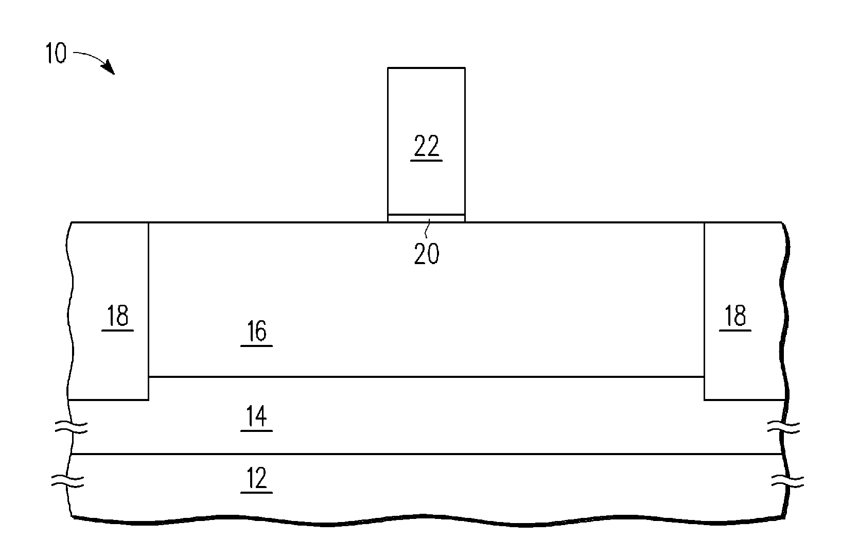
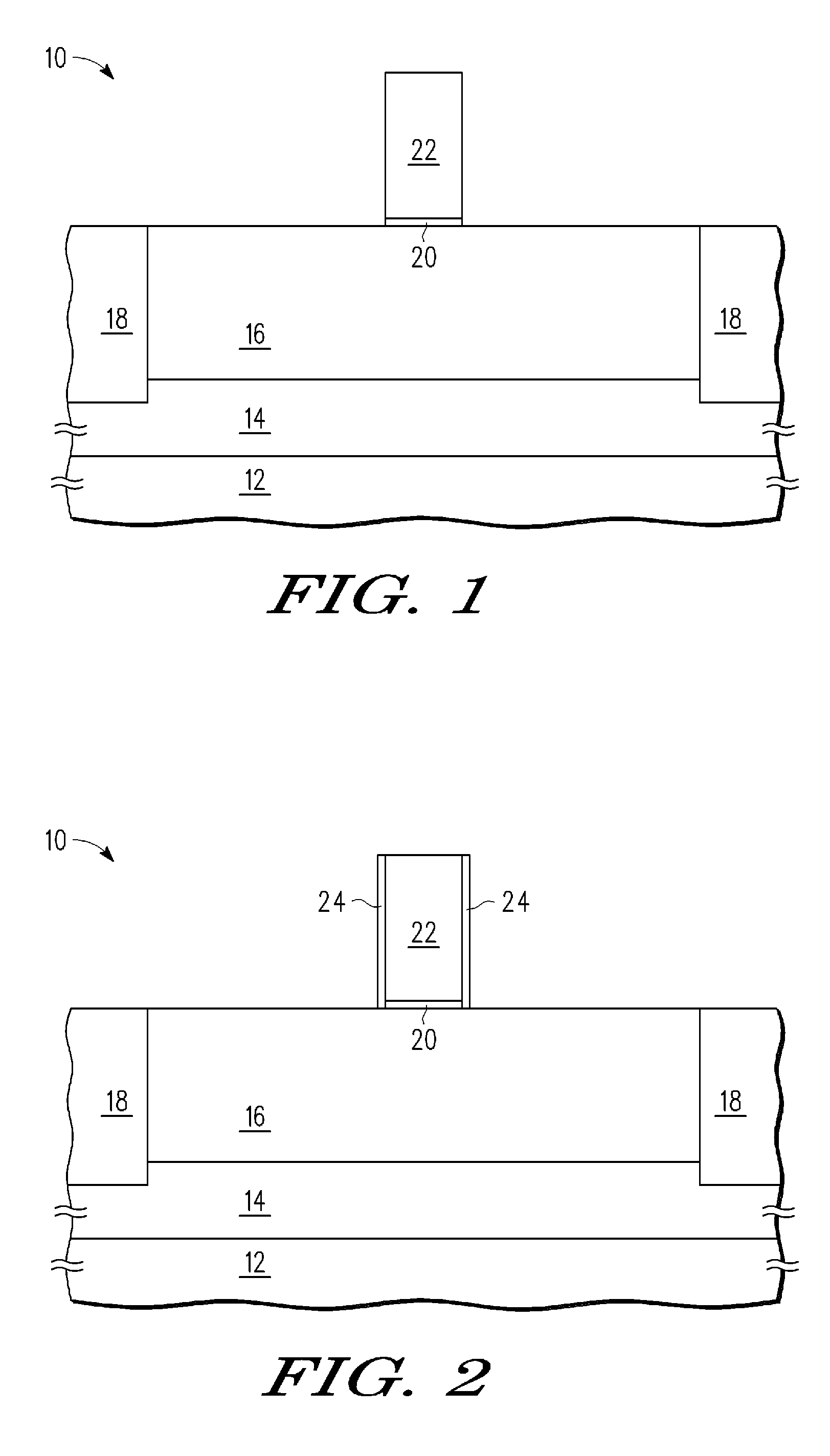
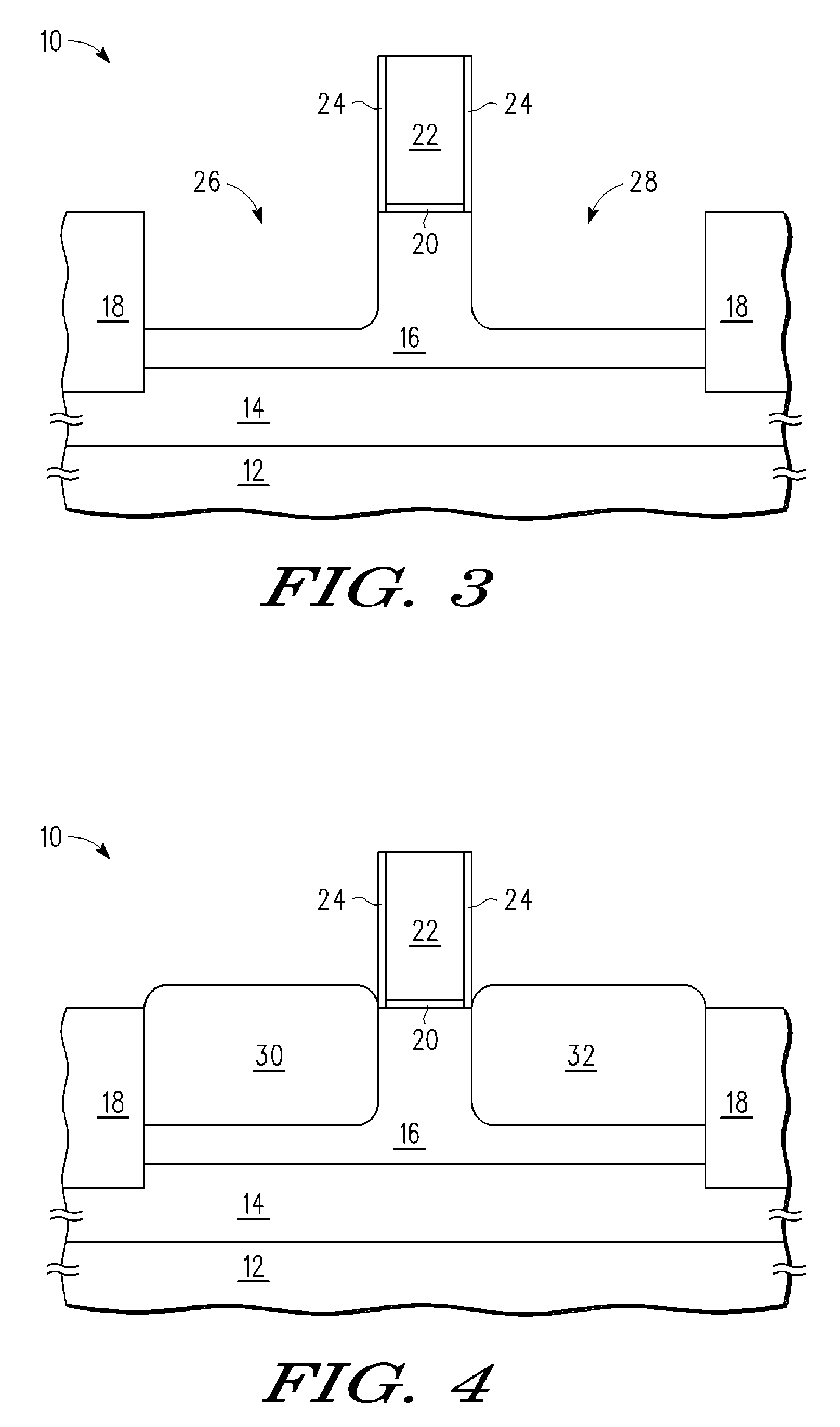
[0017]Semiconductor devices, including method of making the same, are provided. Exemplary semiconductor devices include a structure with a high-k zero spacer, which is aligned with a fully in-situ doped source / drain extension stressor. The etching step to form the recesses in which the in-situ doped epitaxial regions are formed is defined using the high-k spacer, as a mask.

[0018]In one aspect, a method for forming a semiconductor device is provided. The method includes forming a semiconductor layer and forming a gate structure overlying the semiconductor layer. The method further includes forming a high-k sidewall spacer adjacent to the gate structure. The method further includes forming a recess in the semiconductor layer, the recess aligned to the high-k sidewall spacer. The method further includes forming an in-situ doped epitaxial material in the recess, the epitaxial material having a natural lattice constant different from a lattice constant of the semiconductor layer to creat...


PUM

PropertyMeasurementUnit
dielectric constantaaaaaaaaaa
widthaaaaaaaaaa
widthaaaaaaaaaa

Abstract

A method for forming a semiconductor device is provided. The method includes forming a semiconductor layer. The method further includes forming a gate structure overlying the semiconductor layer. The method further includes forming a high-k sidewall spacer adjacent to the gate structure. The method further includes forming a recess in the semiconductor layer, the recess aligned to the high-k sidewall spacer. The method further includes forming an in-situ doped epitaxial material in the recess, the epitaxial material having a natural lattice constant different from a lattice constant of the semiconductor layer to create stress in a channel region of the semiconductor device.

Description

BACKGROUND[0001]1. Field[0002]This disclosure relates generally to semiconductor devices, and more specifically, to source / drain stressors formed using in-situ epitaxial growth.[0003]2. Related Art[0004]To obtain high channel strain from source / drain stressors, the source / drain stressors should be incorporated as close as possible to the channel. When source / drain stressors are grown epitaxially in recesses adjacent to the gate, the recesses require a hydrofluoric acid clean (HF clean) prior to the growth of the source / drain stressors. The materials used for HF clean can, however, attack the gate oxide. To prevent the negative effect of HF clean on gate oxide, the source / drain stressors must be formed at some distance from the channel. Separation between the source / drain region and the channel region creates high series resistance.[0005]Conventionally, the high series resistance in the source / drain region has been reduced by implanting dopants in the source / drain region and annealin...

Claims


Application Information

Patent Timeline
Patent Type & Authority Patents(United States)
IPC IPC(8): H01L21/335
CPCH01L29/6653H01L29/66628H01L29/66636H01L29/7848H01L29/165H01L29/517H01L29/665H01L29/78
Inventor WINSTEAD, BRIAN A.TRIVEDI, VISHAL P.ZHANG, DA
Owner NXP USA INC
Features
  • R&D
  • Intellectual Property
  • Life Sciences
  • Materials
  • Tech Scout
  • Unparalleled Data Quality
  • Higher Quality Content
  • 60% Fewer Hallucinations
Learn More