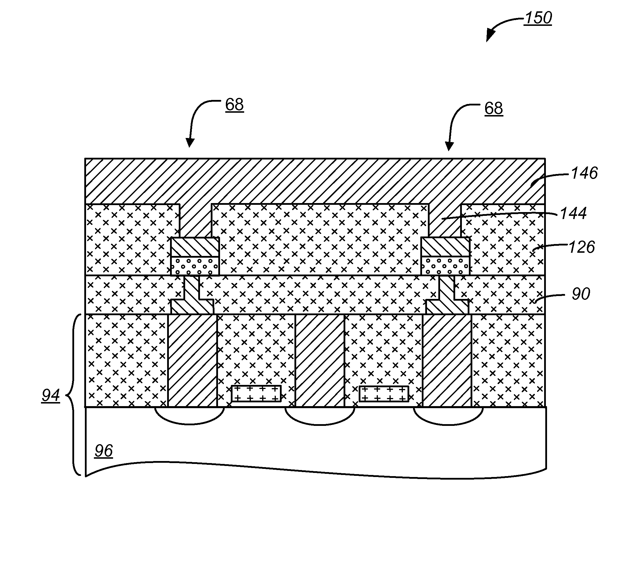
Memory cell with memory element contacting an inverted T-shaped bottom electrode
a memory cell and bottom electrode technology, applied in the direction of digital storage, semiconductor/solid-state device details, instruments, etc., can solve the problems of low efficiency, low efficiency, and inability to meet the requirements of large-scale, and achieve the effect of reducing the amount of current needed, reducing the magnitude of current, and improving adhesion
- Summary
- Abstract
- Description
- Claims
- Application Information
AI Technical Summary
Benefits of technology
Problems solved by technology
Method used
Image

Examples
Embodiment Construction
The following description of the invention will typically be with reference to specific structural embodiments and methods. It is to be understood that there is no intention to limit the invention to the specifically disclosed embodiments and methods but that the invention may be practiced using other features, elements, methods and embodiments. Preferred embodiments are described to illustrate the present invention, not to limit its scope, which is defined by the claims. Those of ordinary skill in the art will recognize a variety of equivalent variations on the description that follows. Like elements in various embodiments are commonly referred to with like reference numerals.
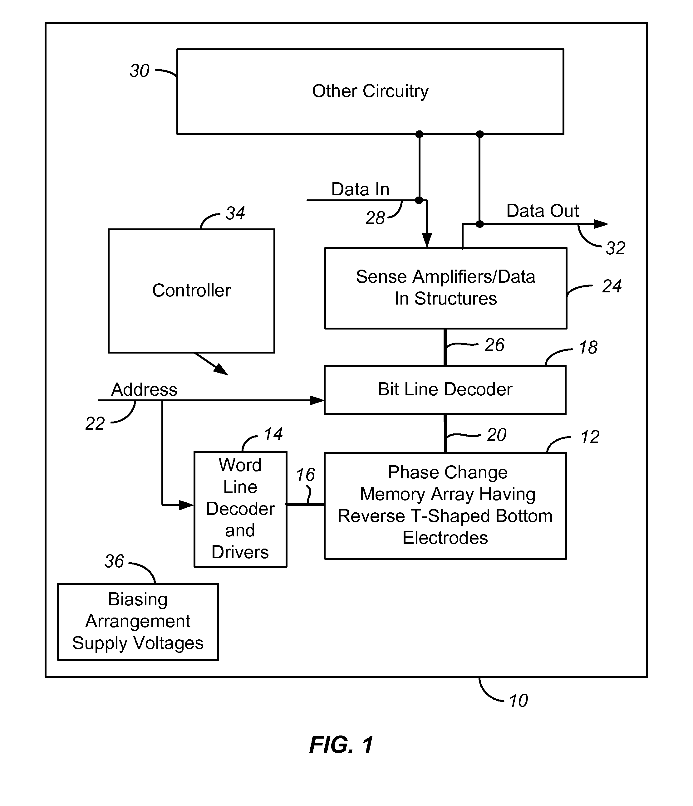
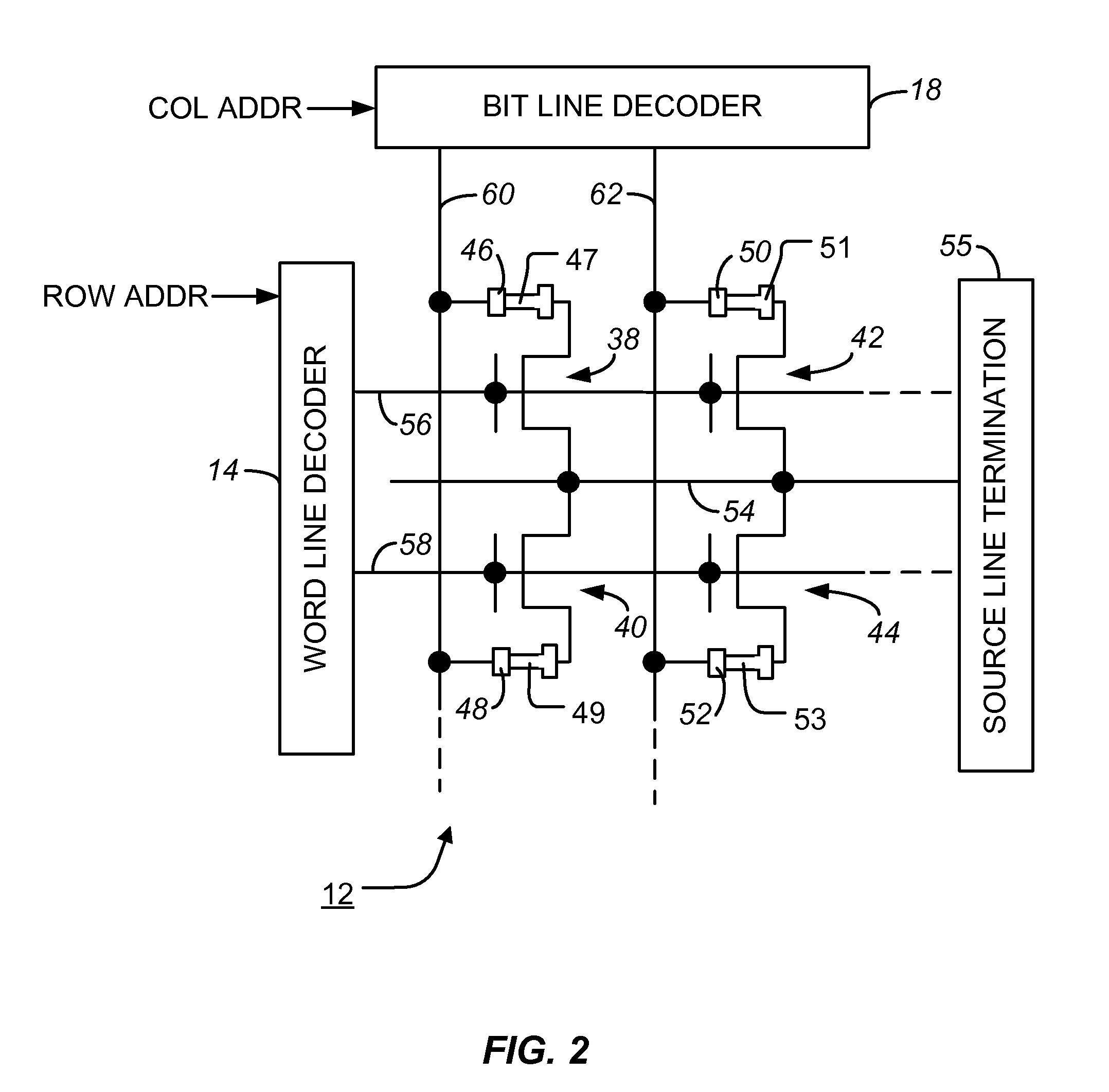
FIG. 1 is a simplified block diagram of an integrated circuit 10 including a memory array 12 implemented using memory cells as described herein having inverted T-shaped bottom electrodes. A word line decoder 14 is coupled to and in electrical communication with a plurality of word lines 16. A bit line (column)...
PUM
 Abstract
Description
Claims
Application Information
 - R&D
- Intellectual Property
- Life Sciences
- Materials
- Tech Scout
- Unparalleled Data Quality
- Higher Quality Content
- 60% Fewer Hallucinations
Browse by: Latest US Patents, China's latest patents, Technical Efficacy Thesaurus, Application Domain, Technology Topic, Popular Technical Reports.
© 2025 PatSnap. All rights reserved.Legal|Privacy policy|Modern Slavery Act Transparency Statement|Sitemap|About US| Contact US: help@patsnap.com