

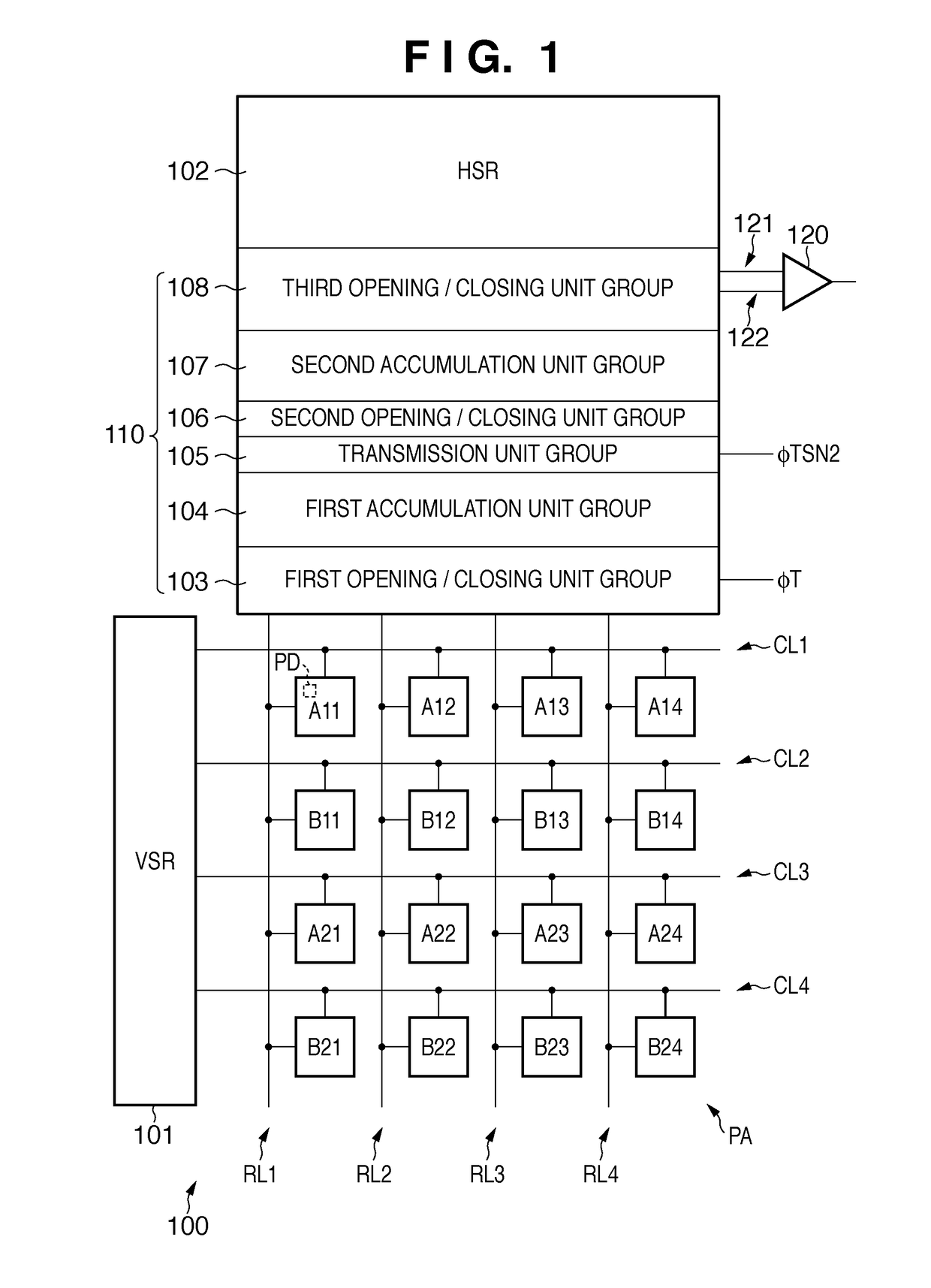
Image sensing apparatus and imaging system
a technology of image sensing apparatus and image sensor, which is applied in the direction of color television details, television system details, television systems, etc., can solve the problems of increasing chip area and increasing the entire power consumption of the image sensing apparatus in the readout period, so as to suppress the increase in power consumption and reduce the chip area
- Summary
- Abstract
- Description
- Claims
- Application Information
AI Technical Summary
Benefits of technology
Problems solved by technology
Method used
Image

Examples
first embodiment
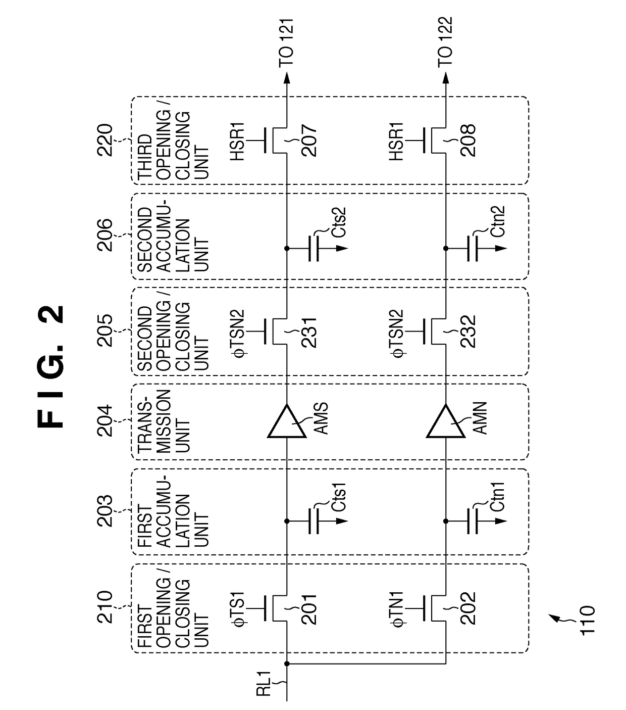
[0091]The transmission unit 504 including the optical signal source follower SFs and noise signal source follower SFn can raise the input impedance and lower the output impedance by the simple arrangement. The transmission unit 504 supplies a signal corresponding to electric charges held by the first accumulation unit 203 to the second accumulation unit 206, instead of directly supplying the electric charges held by the first accumulation unit 203 themselves to the second accumulation unit 206, as in the
[0092]Each of the optical signal source follower SFs and noise signal source follower SFn of the transmission unit 504 may include a PMOS transistor in place of the NMOS transistor (MOS transistor MS or MN).
[0093]An image sensing apparatus 600 according to the third embodiment of the present invention will be described next with reference to FIGS. 8 to 11. FIG. 8 is a view showing the arrangement of the image sensing apparatus 600 according to the third embodiment of the present inve...
third embodiment
[0126]In the third embodiment, the transmission unit 504 transmits the noise signal and optical signal to the second accumulation unit 206 via the separate source followers SFs and SFn. For this reason, variations between the source followers SFs and SFn produce fixed pattern noise that degrades the image quality. That is, the noise signal and optical signal held by the second accumulation unit 206 contain different source follower offsets. More specifically, since the threshold voltage of the NMOS transistor MS of the source follower SFs is different from that of the NMOS transistor MN of the source follower SFn, offset noise cannot be removed by calculating the difference between the noise signal and the optical signal, and fixed pattern noise remains. The fixed pattern noise varies between the columns and therefore generates vertical stripe-shaped noise in the image based on the obtained image signal.
fifth embodiment
[0127]In the fifth embodiment, however, a first noise signal accumulation unit Ctn1 or a first optical signal accumulation unit Cts1 is selectively connected to the input terminal of the transmission unit 1304. A second noise signal accumulation unit Ctn2 or a second optical signal accumulation unit Cts2 is selectively connected to the output terminal. More specifically, the first noise signal accumulation unit Ctn1 is connected to the transmission unit 1304 via a noise signal switch 1312, whereas the first optical signal accumulation unit Cts1 is connected via an optical signal switch 1311. The second noise signal accumulation unit Ctn2 is connected to the transmission unit 1304 via a noise signal switch 232, whereas the second optical signal accumulation unit Cts2 is connected via an optical signal switch 231. This allows the transmission unit 1304 to selectively transmit the noise signal or optical signal to a second accumulation unit 206 via a common source follower SFsn. For th...
PUM
 Abstract
Description
Claims
Application Information