
Liquid crystal display

a liquid crystal display and display panel technology, applied in the field of liquid crystal display, can solve the problems of reducing color reproducibility and contrast ratio, and achieve the effect of reducing the alignment error between the display panels and increasing the aperture ratio of the liquid crystal display

Active Publication Date: 2011-03-15
SAMSUNG DISPLAY CO LTD
View PDF17 Cites 4 Cited by
  • Summary
  • Abstract
  • Description
  • Claims
  • Application Information

AI Technical Summary

Benefits of technology

[0013]According to one aspect of the present invention, alignment error between the display panels is reduced and the aperture ratio of the liquid crystal display is increased in a liquid crystal display that includes a first substrate, a color filter formed on the first substrate, a first electrode formed on the color filter, an interlayer insulating layer formed on the first electrode, a light blocking member formed on the interlayer insulating layer and partially overlapped by the first electrode, a second substrate facing the first substrate, a second electrode formed on the second substrate, and a liquid crystal layer interposed between the first and second substrates. The light blocking member and the first electrode may be overlap each other with the interlayer insulating layer interposed therebetween to form a storage capacitor.

Problems solved by technology

Also, misalignment between the pixel electrodes and the color filters and light blocking members may occur in the process of assembling the two display panels of the liquid crystal display to face each other, and the misalignment may decrease color reproducibility and contrast ratio.

Method used


Image

  • Liquid crystal display
  • Liquid crystal display
  • Liquid crystal display

Examples


Embodiment Construction

[0026]In the drawings, the thickness of layers, films, panels, regions, etc., are exaggerated for clarity. Like reference numerals designate like elements throughout the specification. It will be understood that when an element such as a layer, film, region, or substrate is referred to as being “on” another element, it can be directly on the other element or intervening elements may also be present. In contrast, when an element is referred to as being “directly on” another element, there are no intervening elements present.

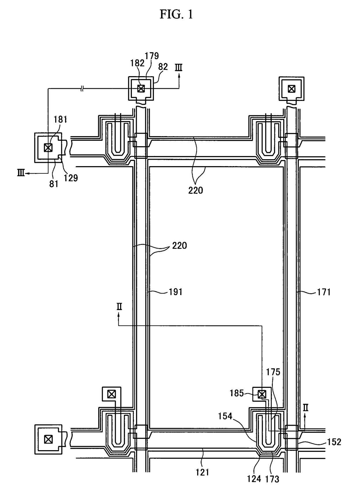
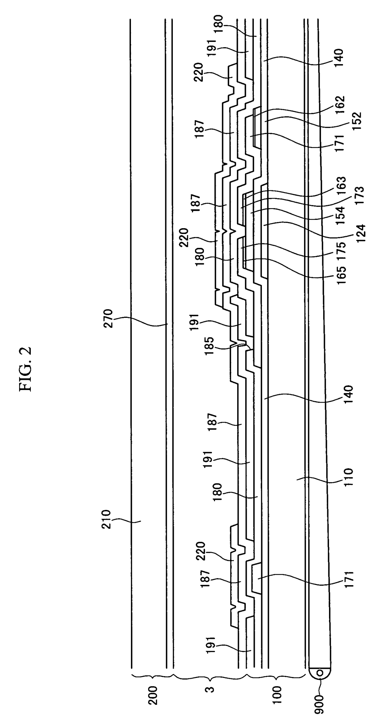
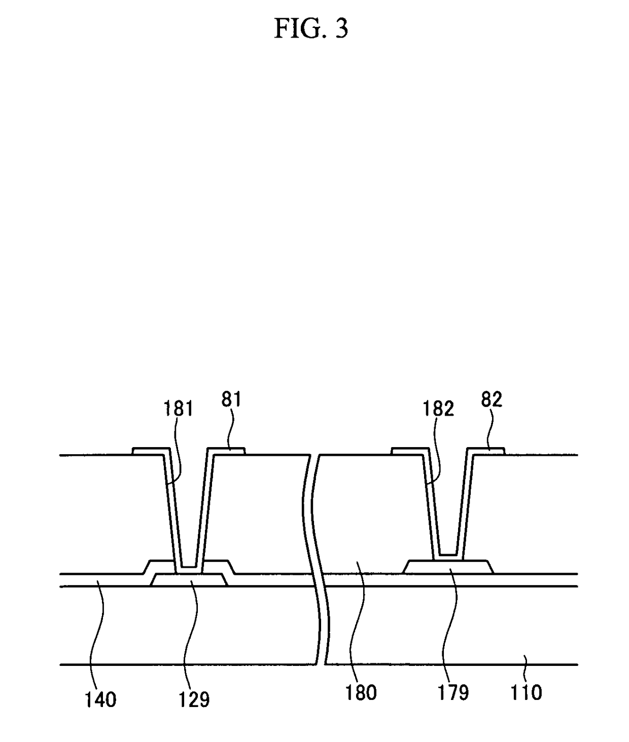
[0027]A liquid crystal display according to an exemplary embodiment of the present invention will now be described in detail with reference to FIG. 1 to FIG. 3.

[0028]FIG. 1 is a layout view of a thin film transistor array panel according to an exemplary embodiment of the present invention, and FIG. 2 and FIG. 3 are cross-sectional views of the thin film transistor array panel taken along lines II-II and III-III of FIG. 1, respectively.

[0029]The liquid crystal disp...


PUM

PropertyMeasurementUnit
inclination angleaaaaaaaaaa
dielectric constantaaaaaaaaaa
conductiveaaaaaaaaaa

Abstract

A liquid crystal display is provided with a first substrate, a color filter formed on the first substrate, a first electrode formed on the color filter, an interlayer insulating layer formed on the first electrode, a light blocking member formed on the interlayer insulating layer and partially overlapping the first electrode, a second substrate facing the first substrate, a second electrode formed on the second substrate, and a liquid crystal layer interposed between the first and second substrates, wherein the light blocking member and the first electrode may be overlap each other, with the interlayer insulating layer interposed therebetween to form a storage capacitor.

Description

CROSS-REFERENCE TO RELATED APPLICATION[0001]This application claims priority to and the benefit of Korean Patent Application No. 10-2006-0015478 filed in the Korean Intellectual Property Office on Feb. 17, 2006, the entire contents of which are incorporated herein by reference.BACKGROUND OF THE INVENTION[0002]1. Field of the Invention[0003]The present invention relates to a liquid crystal display.[0004]2. Description of the Related Art[0005]A liquid crystal display (LCD) includes a pair of display panels having field generating electrodes and polarizers and a liquid crystal layer interposed between the two display panels. Field generating electrodes generate an electric field of varying intensity thereby varying the arrangement of liquid crystal molecules and changing the polarization of light passing through the liquid crystal layer. A polarizer blocks or transmits the polarized light appropriately to make bright and dark regions, thereby displaying desired images.[0006]Color filte...

Claims


Application Information

Patent Timeline
Patent Type & Authority Patents(United States)
IPC IPC(8): G02F1/136G02F1/1333
CPCG02F1/136209G02F1/136213G02F2001/136222G02F1/136222F16M13/027G03B21/145G03B21/54H04N9/3141
Inventor OH, JOON-HAK
Owner SAMSUNG DISPLAY CO LTD
Learn More