Semiconductor device with multiple designation marks

a technology of semiconductor devices and designation marks, applied in semiconductor devices, semiconductor/solid-state device details, electrical apparatus, etc., can solve the problem that the bonding part cannot be freely selected, and achieve the effect of ensuring the connection reliability of the bonding pad and desirable flexibility in selecting the bonding region

Active Publication Date: 2011-04-19
RENESAS ELECTRONICS CORP
View PDF6 Cites 0 Cited by
  • Summary
  • Abstract
  • Description
  • Claims
  • Application Information

AI Technical Summary

Benefits of technology

[0011]As described above, according to the present invention, it is possible to ensure the connection reliability of the bonding pad and provide a semiconductor device with bonding pads having desirable flexibility in selection of the bonding region.

Problems solved by technology

Thus, the bonding part cannot be freely selected after forming the bonding pad.

Method used


Image

  • Semiconductor device with multiple designation marks
  • Semiconductor device with multiple designation marks
  • Semiconductor device with multiple designation marks

Examples


second embodiment

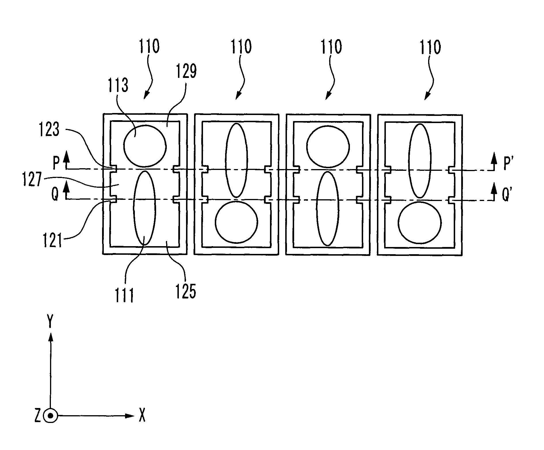
[0076]In the first embodiment, the notches or the protrusions are provided on the depressed portion side wall 157 for the detection of the boundaries. However, the method of forming the mark for indicating the boundaries is not limited to this. For example, the area indication marks may be corners provided at the depressed portion 155. In the configuration in which the corners of the depressed portion 155 are the area indication marks, for example, the third region 127 is pulled in or out from the long side of the rectangle with respect to the first region 125 and the second region 129. In the present embodiment, such configuration will be described.

[0077]FIG. 13 is a plan view showing the configuration of the semiconductor device in the present embodiment. The basic configuration of the semiconductor device 130 shown in FIG. 13 is the same as that of the semiconductor device 100 in the first embodiment (shown in FIG. 5). However, the configuration is different from the semiconducto...


PUM


Abstract

The semiconductor device having a bonding pad is provided. The bonding pad enables highly reliable connection and high flexibility of the selection of the area to be bonded. The semiconductor device includes a bonding pad and an area designation marking. The bonding pad includes a first region, a second region and a third region formed between the first region and the third region. The area designation marking includes a first notch for designating a first boundary of the first region and the third region and a second notch for designation a second boundary of the second region and the third region. Any of the first region and the second region can be used as the region where the scratch formed by a probing process is to be formed.

Description

BACKGROUND OF THE INVENTION[0001]1. Field of the Invention[0002]The present invention relates to a semiconductor device having bonding pads and a manufacturing method thereof.[0003]2. Description of the Related Art[0004]Japanese Laid Open Patent Applications JP-P 2001-338955A and JP-P 2001-177066A disclose bonding techniques of semiconductor devices. In these documents, a bonding pad having a bonding region to which a bonding wire is bonded and a probe contact region to which a test probe contacts is described.[0005]In the document JP-P 2001-338955A, a bonding pad having bonding region 334 and probe contact region 336 as shown in FIG. 1 is described. Also in this document, a bonding pad having a bonding region, a probe contact region, and notches located at the both sides of the boundary between the bonding region and the probe contact region is disclosed.[0006]In the document JP-P 2001-177066A, an integrated circuit device having a bonding pad is disclosed. In this document, a bond...

Claims


Application Information

Patent Timeline
Patent Type & Authority Patents(United States)
IPC IPC(8): H01L23/48
CPCH01L23/544H01L24/03H01L24/05H01L24/06H01L24/48H01L24/49H01L24/45H01L24/85H01L2223/54473H01L2224/04042H01L2224/05552H01L2224/05553H01L2224/05556H01L2224/05624H01L2224/05644H01L2224/05647H01L2224/13124H01L2224/13144H01L2224/13147H01L2224/45124H01L2224/45144H01L2224/45147H01L2224/48465H01L2224/49171H01L2224/49431H01L2924/01004H01L2924/01005H01L2924/01013H01L2924/01014H01L2924/01015H01L2924/01029H01L2924/01033H01L2924/01079H01L2924/14H01L2924/19043H01L2924/01006H01L2224/85H01L2224/48624H01L2224/48644H01L2224/48647H01L2224/48844H01L2224/48847H01L2224/48724H01L2224/48747H01L2224/0401H01L2224/02166H01L2924/00014H01L2924/00H01L2224/48824H01L2224/48744H01L2224/0392
Inventor TANABE, AKIHITO
Owner RENESAS ELECTRONICS CORP
Why Eureka
Try Eureka