
LIDAR system utilizing SOI-based opto-electronic components
a technology of opto-electronic components and lidar systems, applied in the field of lidar systems, can solve the problems of affecting the maximum range over which these devices may be used, and the phased array system is generally too expensive for use in the automotive environment, so as to achieve the effect of low cost and higher reliability
- Summary
- Abstract
- Description
- Claims
- Application Information
AI Technical Summary
Benefits of technology
Problems solved by technology
Method used
Image

Examples
Embodiment Construction
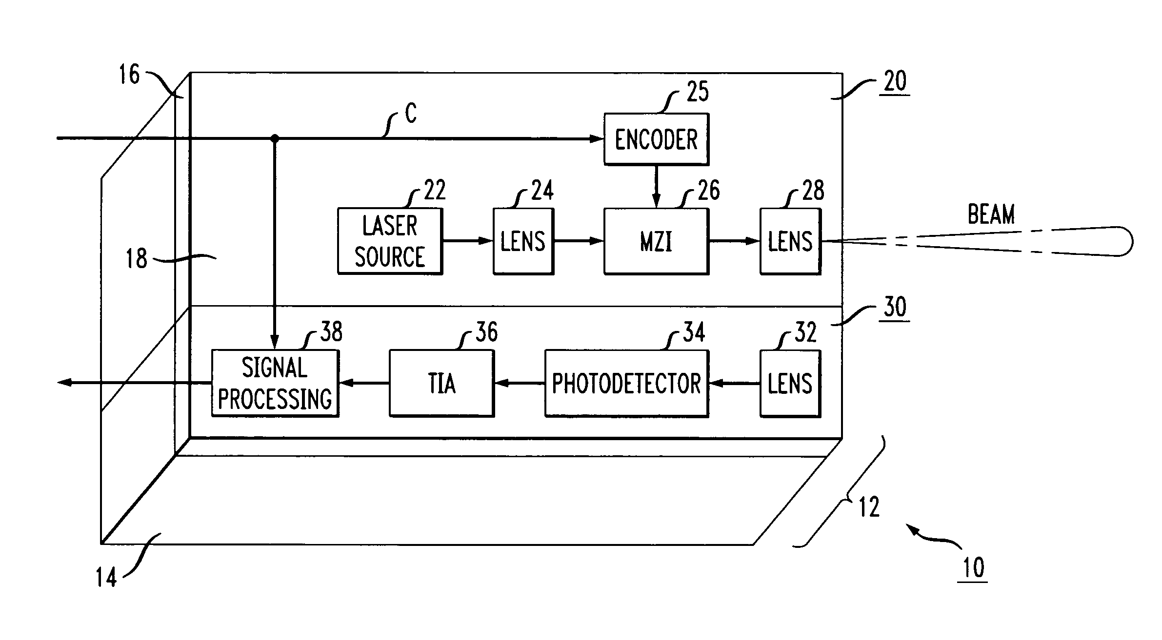
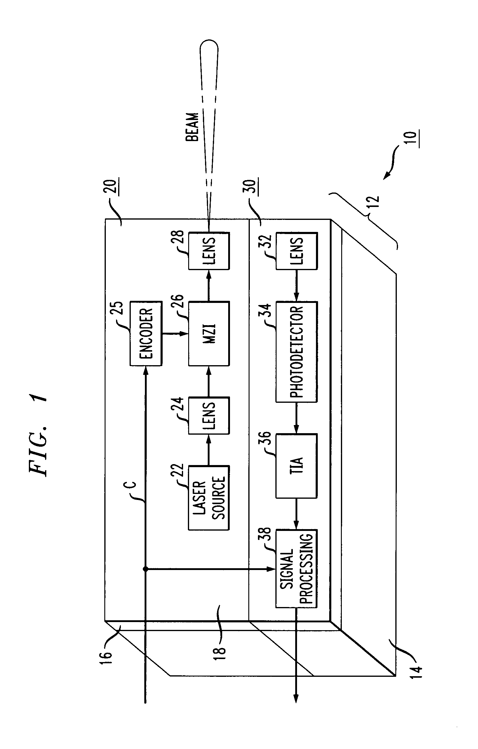
[0025]FIG. 1 illustrates, in an isometric view, an exemplary LIDAR system 10 integrated within an SOI-based platform in accordance with the present invention. In this particular embodiment, the various components of LIDAR system 10 are integrated within a single SOI structure 12. As will be discussed in other examples below, a “multi” module arrangement may also be utilized. Referring to FIG. 1 in particular, however, SOI structure 12 is illustrated as comprising a silicon substrate 14, an overlying insulating layer 16 (formed of a dielectric material, such as silicon dioxide and often referred to as the “buried oxide” layer), and a surface silicon layer 18 (hereinafter referred to as the “SOI layer”), where SOI layer 18 is generally of a sub-micron thickness.
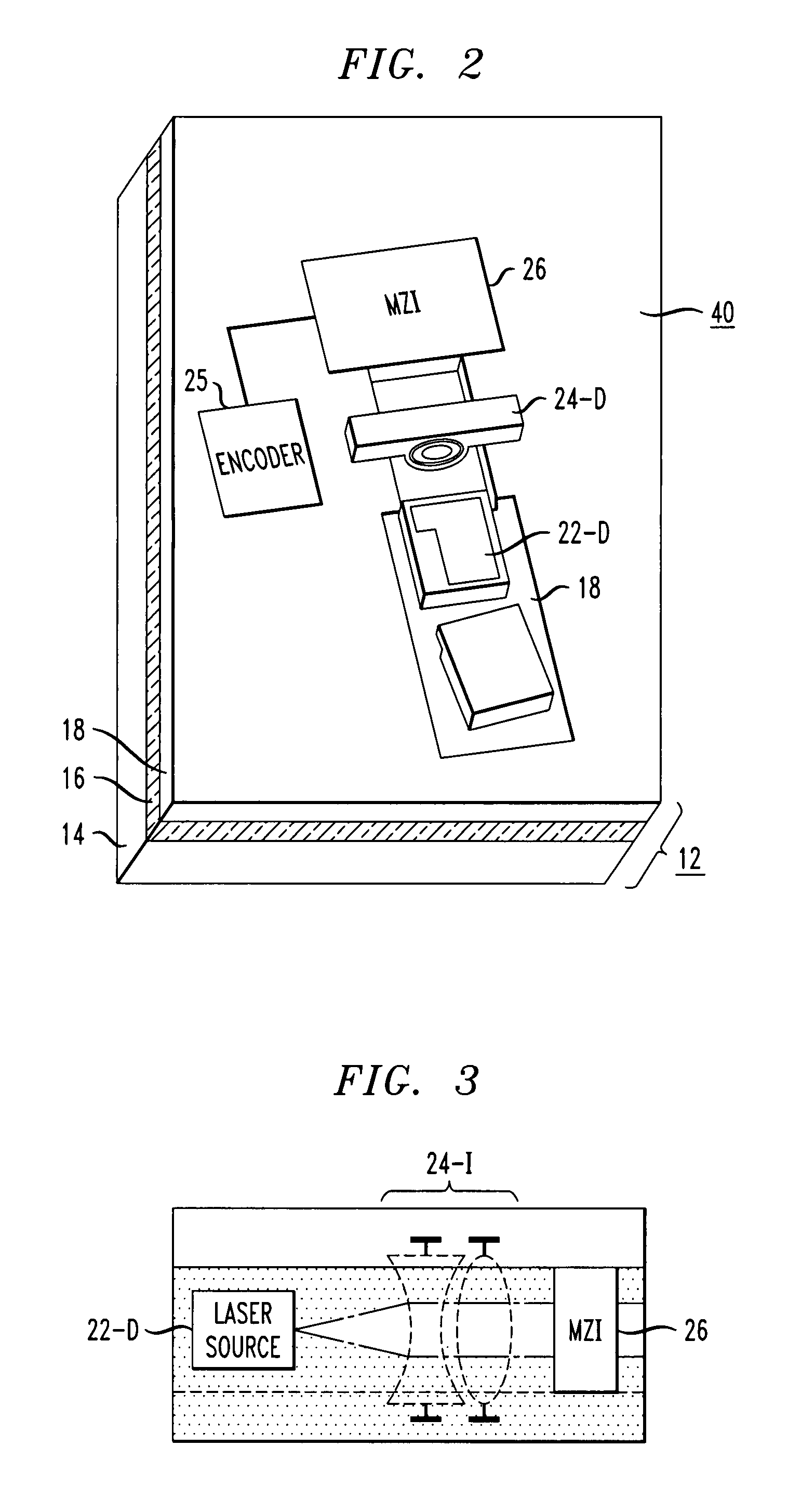
[0026]LIDAR system 10 includes a LIDAR transmitter 20 and a LIDAR receiver 30, as shown in FIG. 1. LIDAR transmitter 20 includes a laser source 22, a focusing lens 24, an optical modulator 26 (such as, for example, a Mach-Zehnd...
PUM
 Abstract
Description
Claims
Application Information