Data processing device comprising ADC unit

a data processing device and data processing technology, applied in the field of data processing devices, can solve the problems of complex process of ep 1,233,615 a1 and lack of reliability, and achieve the effect of efficiently suppressing signal artifacts

Active Publication Date: 2011-05-17
NXP BV
View PDF19 Cites 11 Cited by
  • Summary
  • Abstract
  • Description
  • Claims
  • Application Information

AI Technical Summary

Benefits of technology

[0018]The term “digital signal processing unit” (DSP unit) may particularly denote any circuitry or procedure being capable of processing several digital signal portions to generate or assemble a global digital output signal. This processing may include constructing the global digital output signal based on contributions of the input signals in accordance with an algorithm. When the digital signal processing unit is aware of the signal conditioning characteristic and / or of the analog to digital converting capabilities and limitations of the corresponding upstream located entities, a signal reconstruction scheme may be made particularly efficiently.
[0048]A value of the full scale range of the analog to digital converting unit coupled to the first amplifier may be smaller than a value of a full scale range of the analog to digital converting unit coupled to the second amplifier, and simultaneously a resolution of the analog to digital converting unit coupled to the first amplifier may be larger than a resolution of the analog to digital converting unit coupled to the second amplifier. In other words, one ADC may cover a large range of amplitudes but may have a small resolution, and the other one may have a larger resolution but may only cover a small range. The combination of such ADCs may allow to process even high amplitude analog input signals with high accuracy and with acceptable requirements regarding the quality of the ADC units. This may be particularly suitable for processing essentially Gaussian shaped signals.

Problems solved by technology

However, the procedure of EP 1,233,615 A1 may be complex and may lack reliability.

Method used


Image

  • Data processing device comprising ADC unit
  • Data processing device comprising ADC unit
  • Data processing device comprising ADC unit

Examples


Embodiment Construction

[0065]The illustration in the drawing is schematical. In different drawings, similar or identical elements are provided with the same reference signs.

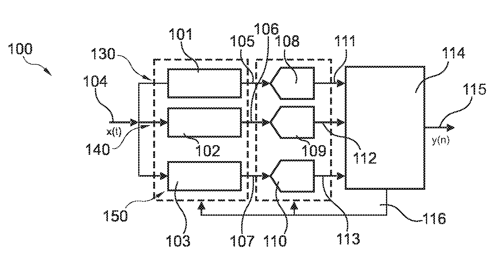
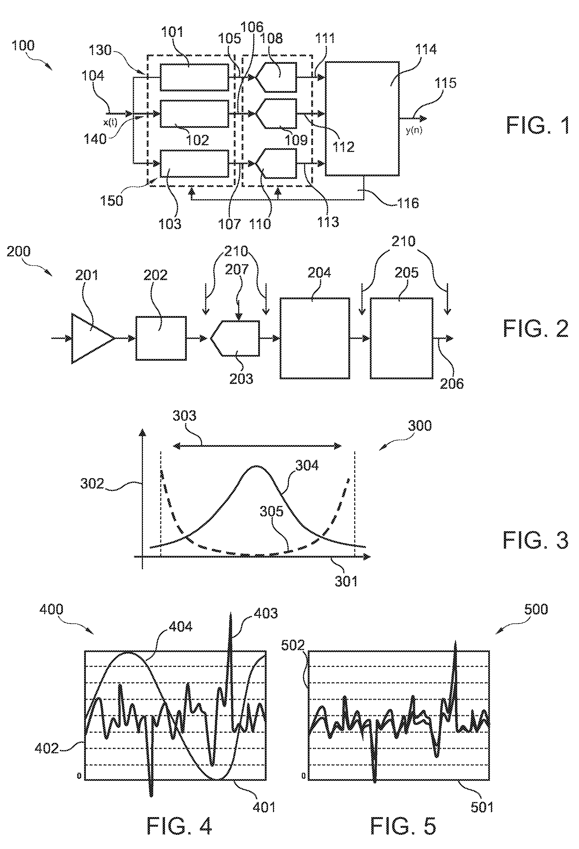
[0066]In the following, referring to FIG. 1, a device 100 for processing data according to an exemplary embodiment of the invention will be explained.

[0067]The device comprises a first signal path 130, a second signal path 140 and a third signal path 150, wherein the signal paths 130, 140, 150 are connected in parallel.

[0068]The device 100 comprises a plurality of signal conditioning units 101 to 103 each receiving an identical analog input signal 104, wherein each of the plurality of signal conditioning units 101 to 103 is adapted for generating a respective analog intermediate signal 105 to 107 by manipulating an amplitude of the analog input signal 104.

[0069]A plurality of analog to digital converting units 108 to 110 are provided each of which being assigned to a corresponding one of the plurality of signal conditioning units 101 t...


PUM


Abstract

A device (100) for processing data, the device (100) comprising a plurality of signal paths (130, 140, 150) each receiving an identical analog input signal (104), at least one signal conditioning unit (101 to 103) in at least one of the plurality of signal paths (130, 140, 150), wherein each signal conditioning unit (101 to 103) is adapted for generating a respective analog intermediate signal (105 to 107) by manipulating a property, particularly an amplitude, of the analog input signal (104), and a plurality of analog to digital converting units (108 to 110) each of which being assigned to a corresponding one of the plurality of signal paths (130, 140, 150) and being supplied with the analog input signal (104) or a respective analog intermediate signal (105 to 107), wherein each of the plurality of analog to digital converting units (108 to 110) is adapted for generating a respective digital intermediate signal (111 to 113) based on the respective analog intermediate signal (105 to 107) or based on the analog input signal (104); a digital signal processing unit (114) supplied with the plurality of digital intermediate signals (111 to 113) and adapted for generating a digital output signal (115) by processing the digital intermediate signals (111 to 113).

Description

FIELD OF THE INVENTION[0001]The invention relates to a device for processing data.[0002]Moreover, the invention relates to method of processing data.[0003]Beyond this, the invention relates to a program element.[0004]Further, the invention relates to a computer-readable medium.BACKGROUND OF THE INVENTION[0005]In electronics, an analog-to-digital converter (ADC) may be denoted as a device for converting an analog signal to a digital (usually binary) code. Simple switches, a network of resistors, current sources or capacitors may implement this conversion.[0006]For instance when transmitting signals between a transmitter and a receiver, an ADC operation may be necessary at the side of the receiver.[0007]EP 1,233,615 A1 discloses to minimize an analog / digital converter over-dimensioning within the framework of reception of signals originating from a satellite and exhibiting power levels that can vary over time. A technique of automatic gain control is disclosed by EP 1,233,615 A1, whic...

Claims


Application Information

Patent Timeline
Patent Type & Authority Patents(United States)
IPC IPC(8): H03M1/00
CPCH03M1/188
Inventor DORIS, KONSTANTINOS
Owner NXP BV
Why Eureka
Try Eureka