

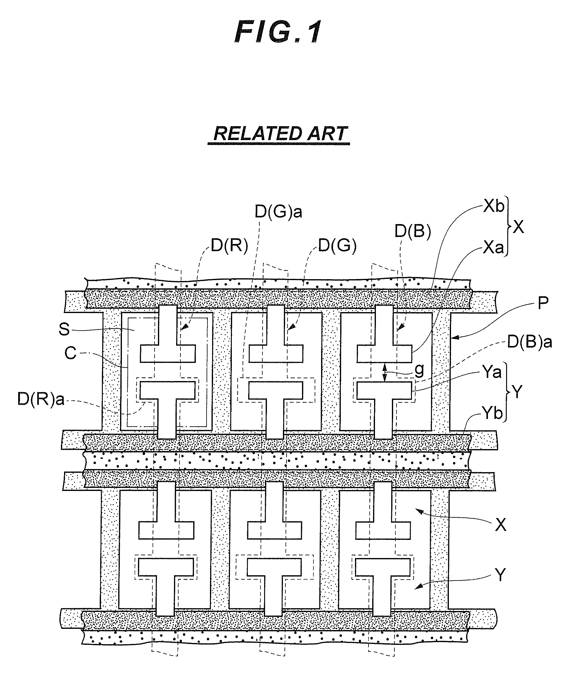
Plasma display panel comprising enhanced discharge on unit light emission area
a technology of alternating current and display panel, which is applied in the direction of gas discharge vessel/container, gas-filled discharge tube, electrode, etc., can solve the problems of increasing electrostatic capacity and discharge voltage, and achieve the effect of facilitating equalization of discharge voltag
- Summary
- Abstract
- Description
- Claims
- Application Information
AI Technical Summary
Benefits of technology
Problems solved by technology
Method used
Image

Examples
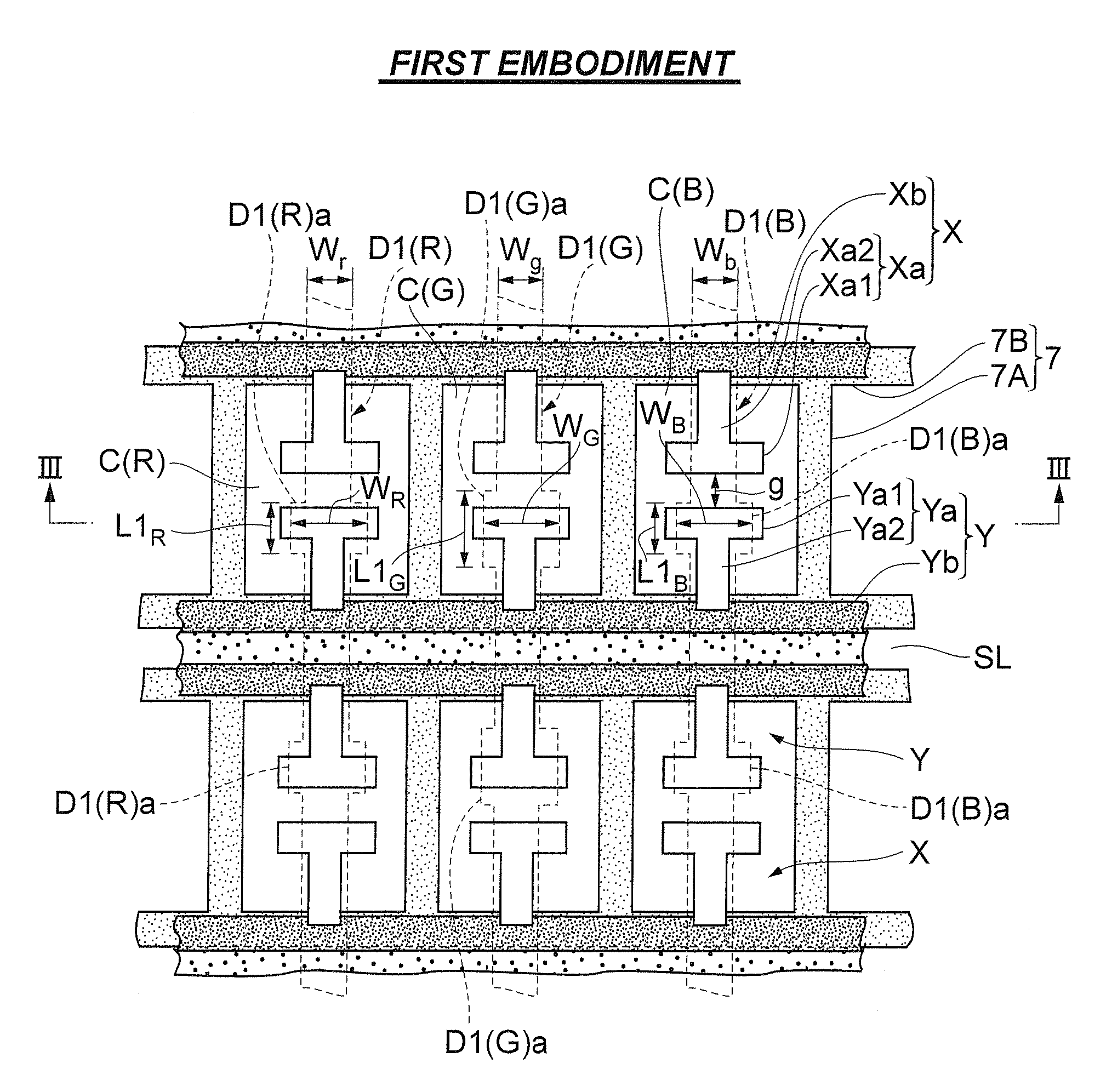
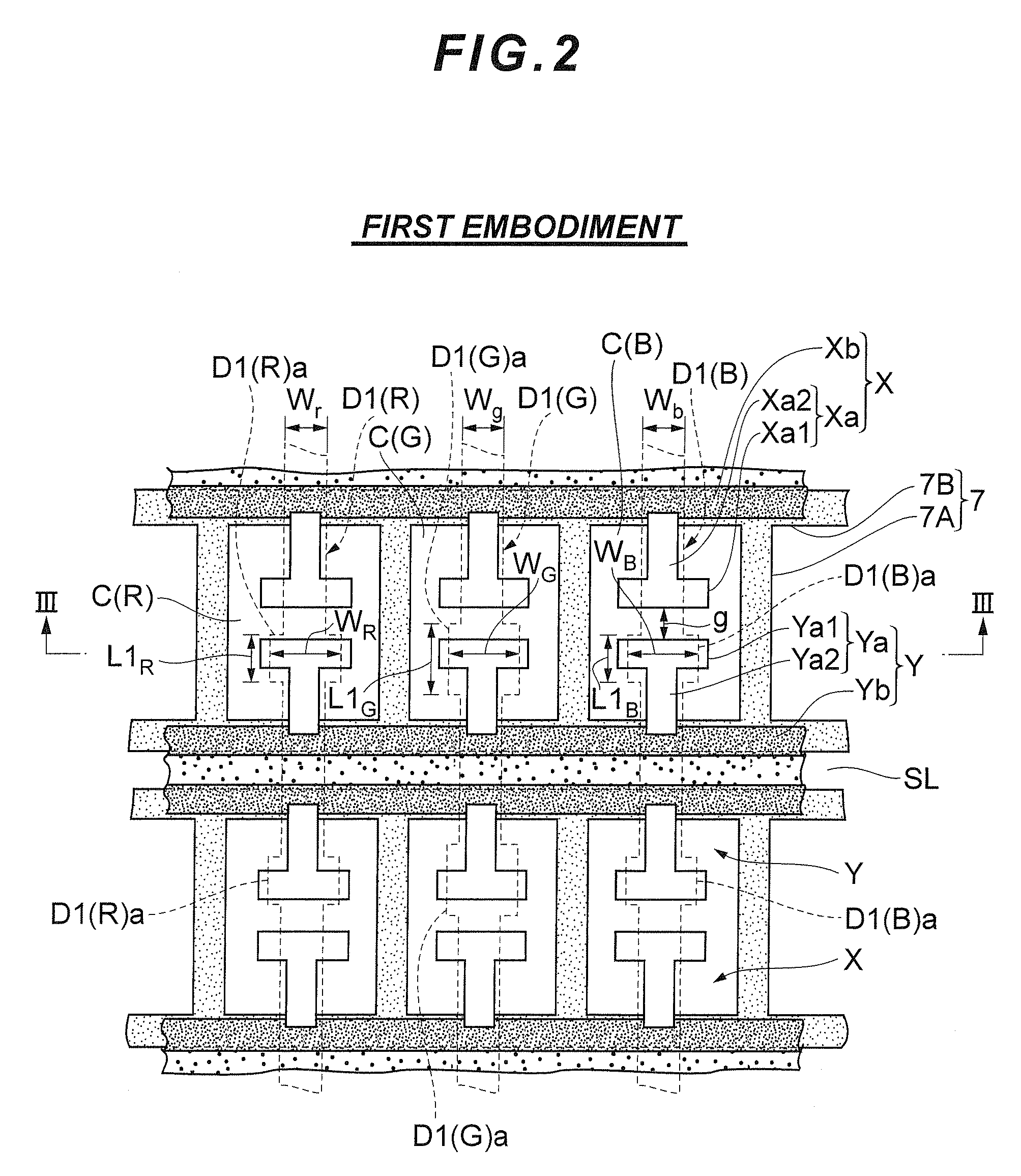
first embodiment
The first embodiment has described the case of the green phosphor layer formed of phosphor materials that make it most difficult for the address discharge to occur, but is applicable to a PDP equipped with the red phosphor layer or the blue phosphor layer formed of phosphor materials that make it most difficult for the address discharge to occur.
The first embodiment has described a PDP employing approximately ladder-shaped partition wall units by way of example, but is applicable to a PDP employing any type of the partition wall unit, such as an approximately grid-shaped partition wall unit and partition walls of a striped shape extending in the column direction.
The first embodiment has described a PDP comprising row electrodes each having island-shaped transparent electrodes extending out from the bus electrode in the column direction in individual discharge cells, by way of example, but is applicable to a PDP comprising row electrodes each having a transparent electrode of a strip...
second embodiment
The second embodiment has described the case of the green phosphor layer formed of phosphor materials that make it most difficult for the address discharge to occur and also the blue phosphor layer formed of phosphor materials that make it easiest for the address discharge to occur, byway of example. However, the present invention is not limited to this example, and as a column electrode faces the discharge cell provided with a phosphor layer making it more and more difficult for the address discharge to occur, a widened portion of the column electrode has a larger and larger area.
Third Embodiment
FIG. 5 is a schematic front view illustrating a PDP of a third embodiment of the present invention.
In the PDP described in the first embodiment, the area of the widened portion of the green column electrode is larger than the area of each of the widened portions of the red and blue column electrodes.
By contrast, in the PDP of the third embodiment, the widened portions D3(R)a, D3(G)a and D3(...
third embodiment
The third embodiment has described the case of the green phosphor layer formed of phosphor materials that make it most difficult for the address discharge to occur, by way of example. However, the present invention is not limited to this example, and as a column electrode faces the discharge cell provided with a phosphor layer making it more and more difficult for the address discharge to occur, a widened portion of the column electrode is located closer and closer to a position facing the center of the discharge cell.
In a basic idea of the PDP described in the aforementioned embodiments, a plasma display panel comprises front and back substrates facing each other across a discharge space, a plurality of row electrode pairs that each extend in a row direction and are arranged in column direction on a rear-facing face of the front substrate and each of which is constituted of a pair of row electrodes facing each other across a discharge gap, a plurality of column electrodes which eac...
PUM
 Abstract
Description
Claims
Application Information