

Plasma display panel
a technology of alternating current and display panels, which is applied in the direction of gas discharge vessels/containers, electrodes, gas-filled discharge tubes, etc., can solve the problems of increasing electrostatic capacity and discharge voltage, and achieve the effect of facilitating equalization of discharge voltages
- Summary
- Abstract
- Description
- Claims
- Application Information
AI Technical Summary
Benefits of technology
Problems solved by technology
Method used
Image

Examples
first embodiment
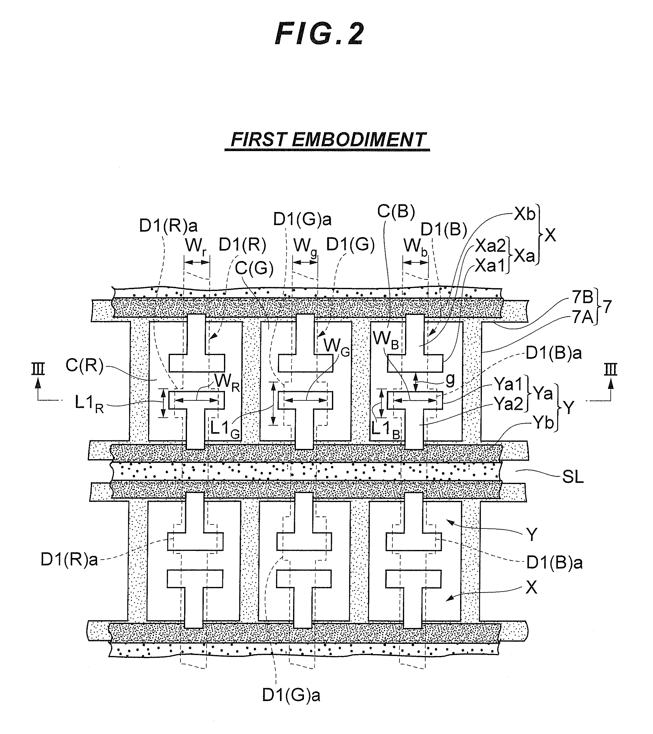
[0035]FIGS. 2 and 3 illustrate a first embodiment of preferred embodiments of the PDP according to the present invention. FIG. 2 is a schematic front view of the PDP of the first embodiment.
[0036]FIG. 3 is a sectional view taken along the III-III line in FIG. 2.
[0037]In FIGS. 2 and 3, a plurality of row electrode pairs (X, Y), which are provided on the inner face (facing the rear of the PDP) of the front glass substrate 1 which serves as the display surface of the PDP, each extend in the row direction (the right-left direction in FIG. 2) and are arranged parallel to each other in the column direction (the up-down direction in FIG. 2).
[0038]Each of the face-to-face row electrodes X, Y constituting each of the row electrode pairs (X, Y) is composed of a plurality of T-shaped transparent electrodes Xa (Ya) and a metal-film-formed bus electrode Xb (Yb) extending in the row direction of the front glass substrate 1. Each of the T-shaped transparent electrodes Xa (Ya) is made up of a widen...
second embodiment
[0072]FIG. 4 is a schematic front view illustrating a PDP of a second embodiment of the present invention.
[0073]In the aforementioned PDP in the first embodiment, the area of the widened portion of the green column electrode is larger than that of each of the widened portions of the red and blue column electrodes, and the widened portions of the red and blue column electrodes are identical in area.
[0074]By contrast, in the PDP of the second embodiment, the area of a widened portion D2(G)a of a green column electrode D2(G) is larger than that of each of the widened portions D2(R)a and D2(B)a of the red and blue column electrodes D2(R) and D2(B).
[0075]In addition to this, the area of the widened portion D2(R)a of the red column electrode D2(R) is greater than the area of the widened portion D2(B)a of the blue column electrode D2(B).
[0076]Specifically, the widened portions D2(R)a, D2(G)a and D2(B)a of the red, green and blue column electrodes D2(R), D2(G) and D2(B) are equal in the row...
third embodiment
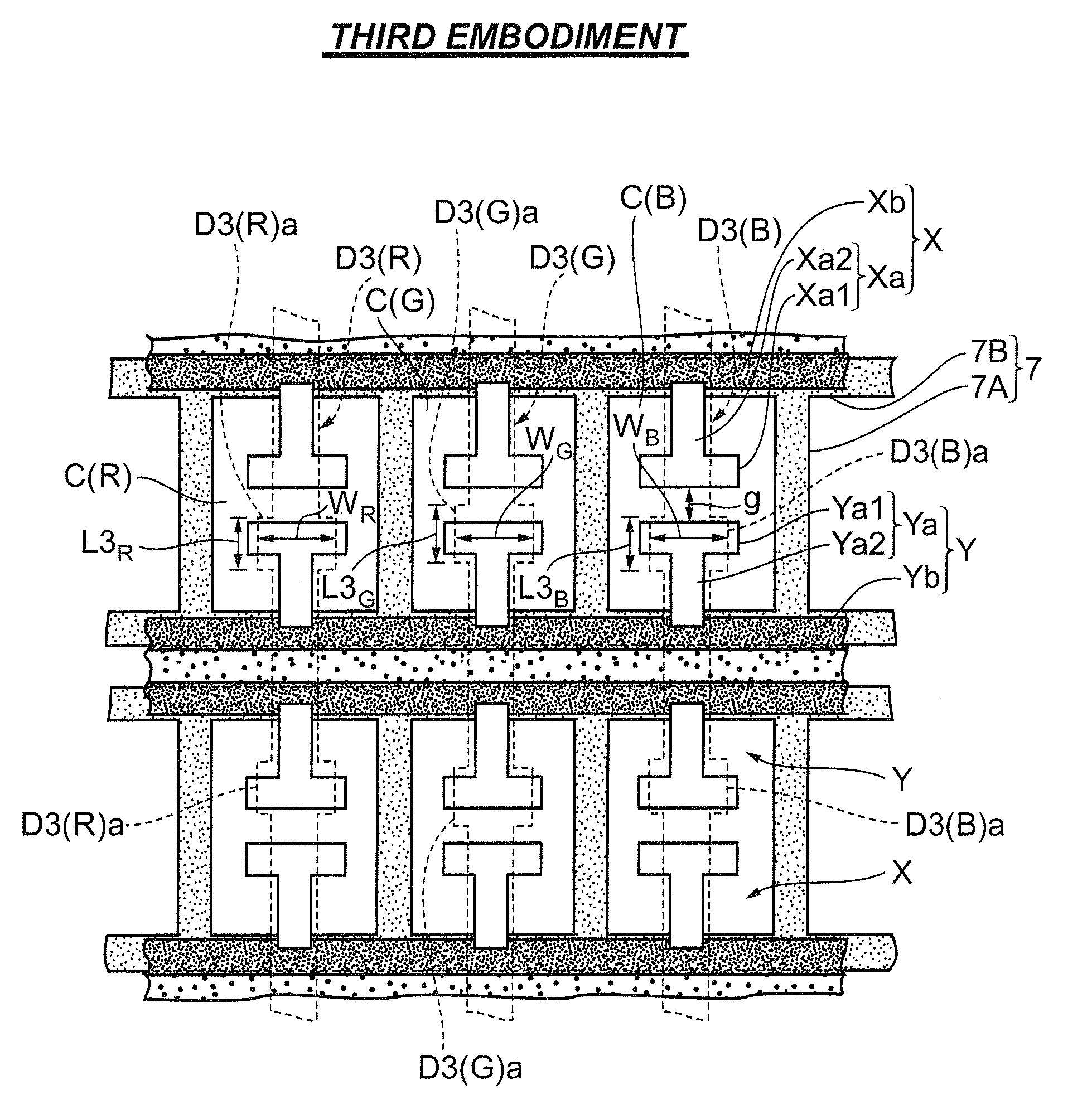
[0086]FIG. 5 is a schematic front view illustrating a PDP of a third embodiment of the present invention.
[0087]In the PDP described in the first embodiment, the area of the widened portion of the green column electrode is larger than the area of each of the widened portions of the red and blue column electrodes.
[0088]By contrast, in the PDP of the third embodiment, the widened portions D3(R)a, D3(G)a and D3(B)a of the respective red, green and blue column electrodes D3(R), D3(G) and D3(B) have equal row-direction widths WR, WG and WB, and equal column-direction lengths L3R, L3G and L3B to each other (WR=WG=WB, L3R=L3G=L3B) so as to be identical in area.
[0089]The widened portion D3(G)a of the green column electrode D3(G) is located closer to a position facing the center of the green discharge cell C(G) in the column direction than the positions of the respective widened portions D3(R)a and D3(B)a of the red and blue column electrodes D3(R) and D3(B) in the red and blue discharge cell...
PUM
 Abstract
Description
Claims
Application Information