
High gain read circuit for 3D integrated pixel

a high gain, read circuit technology, applied in the direction of tv system scanning details, radio frequency control devices, television systems, etc., can solve the problems of increasing reducing the dynamic range of image sensors, and reducing the performance properties of these smaller pixels, so as to reduce the capacitance of floating diffusion, reduce the effect of almost all unwanted electrical coupling and minimizing electrical crosstalk

Active Publication Date: 2011-06-21
OMNIVISION TECH INC
View PDF8 Cites 24 Cited by
  • Summary
  • Abstract
  • Description
  • Claims
  • Application Information

AI Technical Summary

Benefits of technology

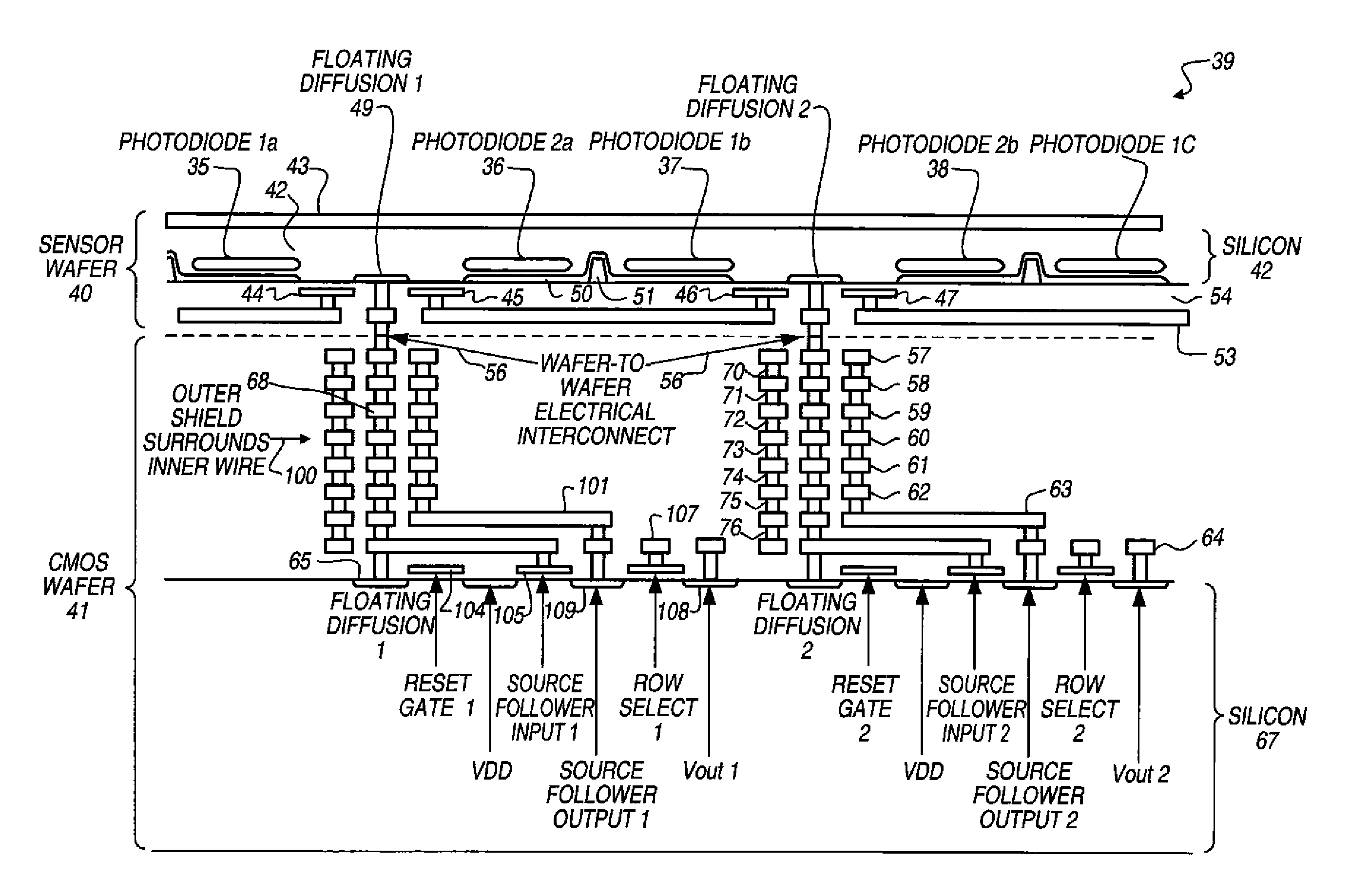
[0010]The present invention is directed to overcoming one or more of the problems set forth above. Briefly summarized, a metal wire interconnecting the floating diffusion on the sensor wafer with the transistors on the circuit wafer is surrounded by a metal shield. The metal shield is connected to an amplifier with gain greater than zero. The output of this amplifier follows the voltage on the floating diffusion node. This reduces the floating diffusion capacitance. The shield also reduces almost all unwanted electrical coupling between adjacent floating diffusions thereby minimizing electrical crosstalk.

Problems solved by technology

In general, as pixels made using CMOS processes scale to smaller dimensions, some performance properties of these smaller pixels degrade.
This reduces the dynamic range of the image sensor.
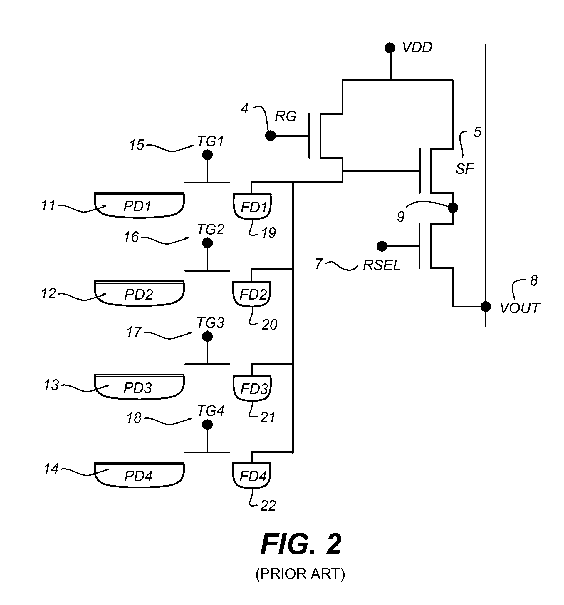
One drawback of shared pixel approach is an increase in the capacitance of the floating diffusions 19, 20, 21, and 22.
Increasing floating diffusion capacitance increases the electron read noise.
Increasing electron read noise reduces dynamic range.
However, one of the negative aspects of this approach is that there is more parasitic floating diffusion capacitance due to the electrical interconnect 55 and electrical interconnect wire 52 between the two wafers.

Method used


Image

  • High gain read circuit for 3D integrated pixel
  • High gain read circuit for 3D integrated pixel
  • High gain read circuit for 3D integrated pixel

Examples


second embodiment

[0028]For most four transistor (4T-pixel) designs, a source follower amplifier, like those shown in FIGS. 1-3, is used to drive the large capacitance of the column circuit. However, the voltage amplification of a source follower circuit is less than one. FIGS. 7 and 8 illustrate a second embodiment that amplifies the voltage applied to the metal shield 100 surrounding the wafer-to-wafer electrical interconnect 68. This reduces the effective capacitance of the floating diffusion 49 and 65. It is noted that this embodiment is the same as FIG. 7 except that a voltage amplifier 120 is attached between the metal shield 100 and the output 109 of the source follower amplifier 105. More specifically, the input of the voltage amplifier 120 is connected to the output 109 of the source follower amplifier 105. Alternatively, the input of the voltage amplifier 120 is connected to the output of the row select transistor 107 (see dashed line). The input voltage to the amplifier 120 needs to be pro...

third embodiment

[0029]FIG. 9 illustrates a This embodiment is the same as FIG. 8 except that a charge pump 111, 140, 141, 142, 143 (the charge pump consists of the elements 111, 140, 141, 142, 143) is substituted for the amplifier 120. Charge pump 111, 140, 141, 142, 143 is small in comparison to other circuits that use operational amplifiers. This provides a gain of greater than 1, and does not require an operational amplifier. The timing for switching transistors phi_1141, phi_2142, and phi_3143 is shown in FIG. 10. When charge is transferred to the floating diffusion 49 and 65, phi_1141 and phi_3143 are on, and phi_2142 off. Assuming the gain of the source follower transistor is 1 then the initial output voltage from the source follower amplifier 105 is QFD / CFD where QFD is the charge on the floating diffusion node, and CFD is the effective floating diffusion capacitance not including the capacitance to the shield. Next, the voltage on the shield is increased using the charge pump. First phi_14...


PUM


Abstract

An image sensor includes (a) a first wafer having (i) a photosensitive area; (ii) a charge-to-voltage conversion region; (b) a second wafer having (i) a first amplifier that receives a signal from the charge-to-voltage conversion region; (c) an electrical interconnect connecting the charge-to-voltage conversion region to an input of the amplifier; (d) an electrically biased shield at least partially enclosing at least a portion of the electrical interconnect.

Description

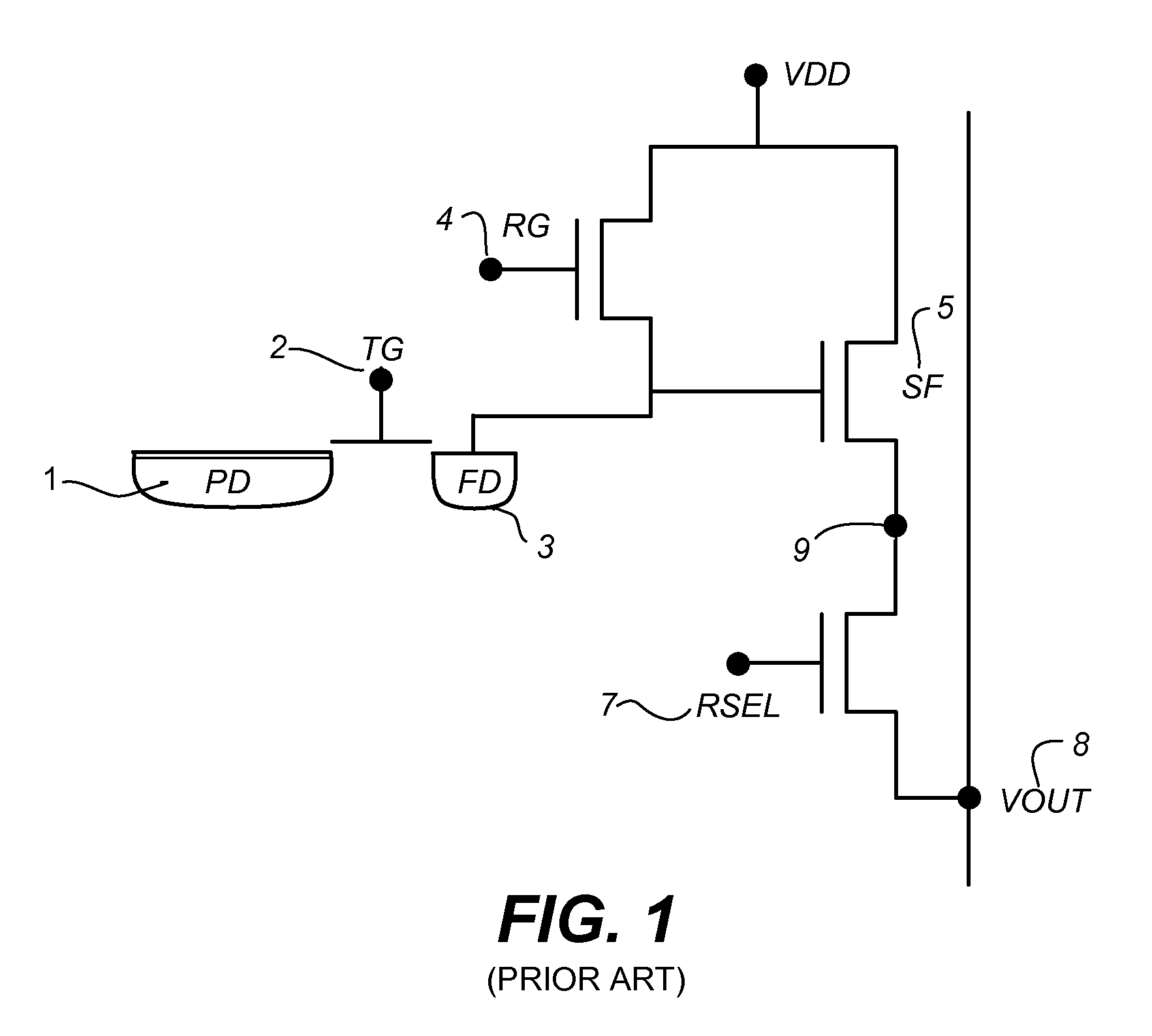
[0001]The present invention relates to CMOS image sensing devices fabricated with active components on two or more wafers, and more specifically, to reducing the amount of signal noise with these types of imaging sensing devices.BACKGROUND OF THE INVENTION[0002]In general, as pixels made using CMOS processes scale to smaller dimensions, some performance properties of these smaller pixels degrade. Specifically, the photodiode capacity decreases. This reduces the dynamic range of the image sensor.[0003]Some of the photodiode capacity can be gained back by moving from a non-shared pixel design as illustrated in FIG. 1 to a shared pixel design like the 4-shared pixel design illustrated in FIG. 2. The non-shared design of FIG. 1 includes a photodiode 1 that collects charge in response to light, and a transfer gate 2 for transferring charge from the photodiode 1 to a floating diffusion 3. A source follower amplifier 5 senses the charge, and in response, the source follower amplifier 5 pas...

Claims


Application Information

Patent Timeline
Patent Type & Authority Patents(United States)
IPC IPC(8): H04N5/335
CPCH01L27/14641H01L27/14636H01L27/14634H01L27/14609H01L2224/80895H01L2224/80896H01L27/146H04N25/62H04N25/77
Inventor MCCARTEN, JOHN P.SUMMA, JOSEPH R.ANDERSON, TODD J.TIVARUS, CRISTIAN A.
Owner OMNIVISION TECH INC
Features
  • Generate Ideas
  • Intellectual Property
  • Life Sciences
  • Materials
  • Tech Scout
  • Unparalleled Data Quality
  • Higher Quality Content
  • 60% Fewer Hallucinations
Learn More