Micromachine MEMS switch

a micromachine switch and switch technology, applied in the direction of waveguide devices, contact surface shapes/structures, electrical apparatus, etc., can solve the problems of poor off isolation characteristic, reduce the capacitive coupling of them, improve the off isolation characteristic of the micromachine switch

Inactive Publication Date: 2002-08-13
NEC CORP
View PDF9 Cites 105 Cited by
  • Summary
  • Abstract
  • Description
  • Claims
  • Application Information

AI Technical Summary

Benefits of technology

In order to achieve the above object, the present invention comprises at least two distributed constant lines disposed close to each other, a movable element arranged above the distributed constant lines so as to oppose the distributed constant lines and connecting the distributed constant lines to each other in a high-frequency manner upon contacting the distributed constant lines, and driving means for displacing the movable element by an electrostatic force to bring the movable element into contact with the distributed constant lines, wherein the movable element includes a projection formed by notching at least one end of an edge of the movable element which is located on at least one distributed constant line side, and a width of the projection serving as a length in a direction parallel to the widthwise direction of the distributed constant lines is smaller than a width of each of the distributed constant lines. That is, at least one end of the movable element is notched to form the projection having the width (the length in the direction parallel to the widthwise direction of the distributed constant lines) smaller than that of the distributed constant line, and the projection is made to oppose the distributed constant line. This decreases the opposing area between the movable element and the distributed constant line, thereby reducing the capacitive coupling of them. Therefore, the OFF isolation characteristic of the micromachine switch can be improved. In addition, since the width of the movable element on the gap between the distributed constant lines becomes larger as compared to the case in which a movable element having the rectangular shape and the width smaller than that of the distributed constant line is used, the present invention can obtain ON reflection characteristic better than that in the above case.

Problems solved by technology

That is, in the conventional micromachine switch 101, an OFF isolation characteristic is poor.

Method used


Image

  • Micromachine MEMS switch
  • Micromachine MEMS switch
  • Micromachine MEMS switch

Examples


first embodiment

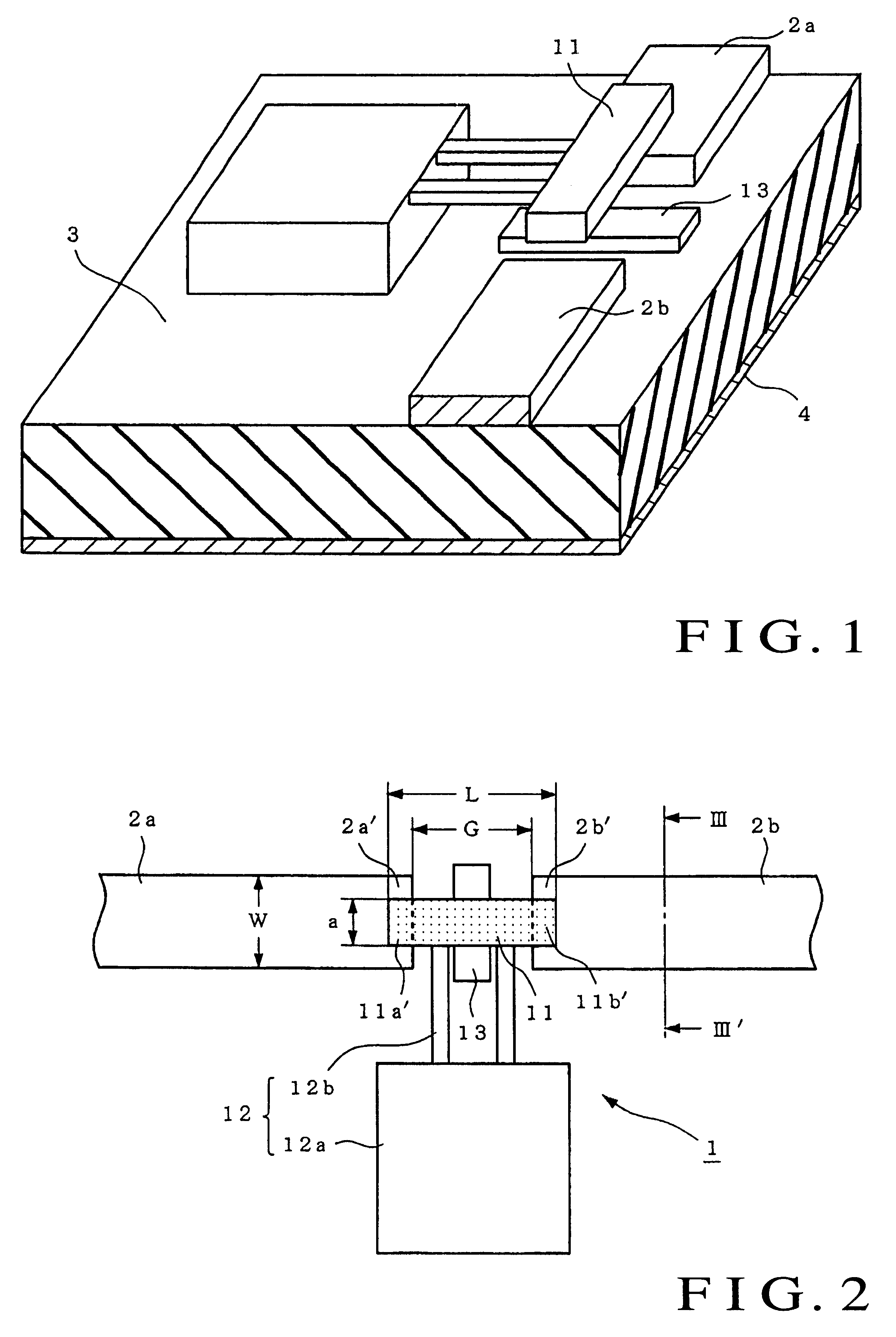
FIG. 1 is a perspective view showing the structure of a micromachine switch according to the first embodiment of the present invention. FIG. 2 is a plan view of the micromachine switch shown in FIG. 1.

As shown in FIG. 1, a micromachine switch 1 is constructed by a switch movable element 11, support means 12, and switch electrode (driving means) 13. The micromachine switch 1 is formed on a dielectric substrate 3 together with two RF microstrip lines (distributed constant lines) 2a and 2b. A GND plate 4 is disposed on the lower surface of the dielectric substrate 3.

The microstrip lines 2a and 2b are closely disposed apart from each other at a gap G. The width of each of both microstrip lines 2a and 2b is W.

The switch electrode 13 is disposed apart between the microstrip lines 2a and 2b on the dielectric substrate 3. The switch electrode 13 is formed to have a height lower than that of each of the microstrip lines 2a and 2b. A driving voltage is selectively applied to the switch electr...

second embodiment

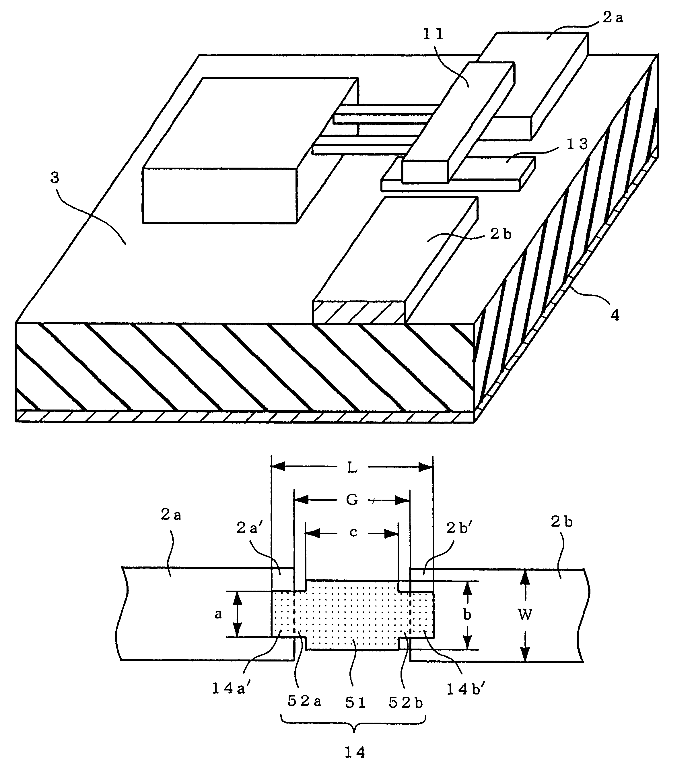
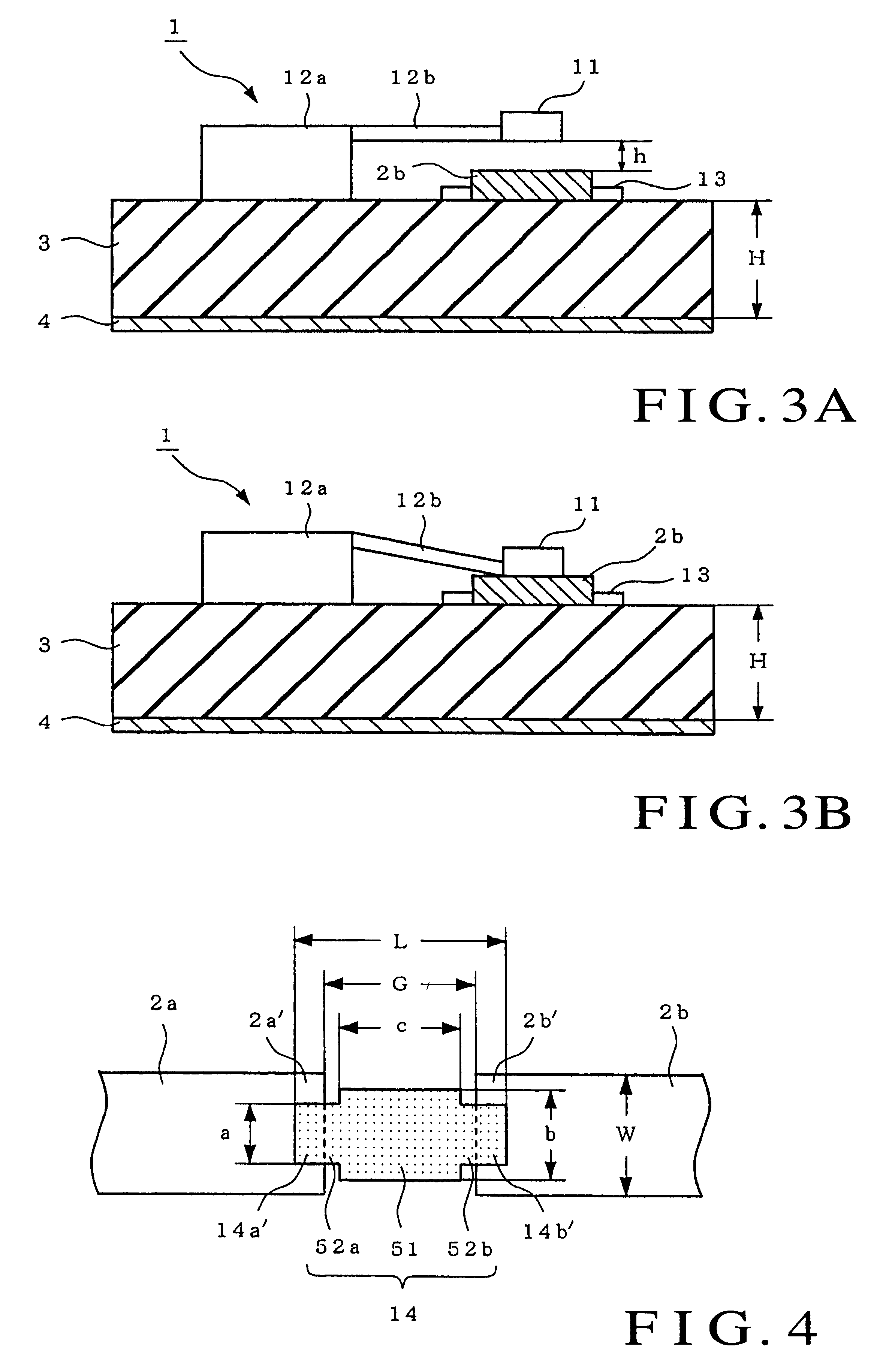
FIG. 4 is a plan view showing the major part of a micromachine switch according to the second embodiment of the present invention. In FIG. 4, the same reference numerals as in FIG. 2 denote the same parts, and a detailed description thereof will be omitted. A switch movable element 14 shown in FIG. 4 is cantilevered on a support means 12, similar to the switch movable element 11 shown in FIG. 2. A switch electrode 13 is disposed at a gap G between microstrip lines 2a and 2b. In FIG. 4, however, the description of the support means 12 and switch electrode 13 is omitted.

This also applies to FIGS. 5 to 9 (to be described later).

A micromachine switch 1 shown in FIG. 4 uses the switch movable element 14 shown in FIG. 4 in place of the switch movable element 11 shown in FIG. 1.

The two ends of an edge of the switch movable element 14 on the microstrip line 2a side are notched to form a projection (second projection) 52a. Similarly, the two ends of the edge of the switch movable element 14 ...

third embodiment

FIG. 7 is a plan view showing the main part of a micromachine switch according to the third embodiment of the present invention. A switch movable element 15 shown in FIG. 7 is different from the switch movable element 14 in FIG. 4 in that a length c of a movable element main body 53 is larger than a gap G, and a width b of the movable element main body 53 is equal to a width W of each of microstrip lines 2a and 2b. In FIG. 7, reference numerals 54a and 54b denote projections (second projections).

Since the length c of the movable element main body 53 is larger than the gap G, the portions of the movable element main body 53 are included in distal end portions 15a' and 15b' of the switch movable element 15. That is, the portions of the movable element main body 53 oppose the microstrip lines 2a and 2b, respectively.

Thus, the opposing area between the switch movable element 15 in FIG. 7 and microstrip lines 2a and 2b becomes larger than that shown in FIG. 4. By using the switch movable...


PUM


Abstract

A switch includes at least two distributed constant lines (2a, 2b) disposed close to each other, a movable element (11) arranged above the distributed constant lines so as to oppose these distributed constant lines and connecting the distributed constant lines to each other in a high-frequency manner upon contacting the distributed constant lines, and a driving means (13) for displacing the movable element by an electrostatic force to bring the movable element into contact with the distributed constant lines. The movable element has a projection (52a, 52b) formed by notching at least one end of an edge of the movable element which is located on at least one distributed constant line side. In this projection, a width (a) serving as a length in a direction parallel to the widthwise direction of the distributed constant lines is smaller than a width (W) of each of the distributed constant lines.

Description

The present invention relates to a micromachine switch used in a milliwave band to microwave band.Switch devices such as a PIN diode switch, HEMT switch, micromachine switch, and the like are used in a milliwave band to microwave band. Of these switches, the micromachine switch is characterized in that the loss is smaller than that of the other devices, and a compact high-integrated switch can be easily realized.FIG. 13 is a perspective view showing the structure of a conventional micromachine switch. FIG. 14 is a plan view of the micromachine switch shown in FIG. 13.A micromachine switch 101 is constructed by a switch movable element 111, support means 112, and switch electrode 113. The micromachine switch 101 is formed on a dielectric substrate 103 together with two RF microstrip lines 102a and 102b. A GND plate 104 is disposed on the lower surface of the dielectric substrate 103.The microstrip lines 102a and 102b are closely disposed apart from each other at a gap G. The switch e...

Claims


Application Information

Patent Timeline
Patent Type & Authority Patents(United States)
IPC IPC(8): H01H59/00H01P1/12H01P1/10H01H1/20H01H1/12H01H1/06
CPCH01H59/0009H01P1/127H01H1/20
Inventor CHEN, SHUGUANG
Owner NEC CORP
Why Eureka
Try Eureka