Driving circuit with impedence calibration

a driving circuit and impedence technology, applied in the direction of pulse generators, electrical apparatus, electric pulse generators, etc., can solve the problems of inability to apply the tail current source connection reference ground, still suffer from an over-large power consumption, etc., and achieve the effect of less power consumption and the same performan

Inactive Publication Date: 2011-08-02
HIMAX IMAGING LIMITED
View PDF23 Cites 15 Cited by
  • Summary
  • Abstract
  • Description
  • Claims
  • Application Information

AI Technical Summary

Benefits of technology

[0007]To solve the abovementioned problems, an exemplary embodiment of the present invention therefore provides a novel driving circuit (e.g., a novel LDVS driver) capable of achieving the same performance with less power consumption.

Problems solved by technology

In this case, a tail current source connecting reference ground is impossible to be applied.
The LDVS driver 300 shown in FIG. 3 can successively meet the requirements of the MIPI standard but still suffers from an over-large power consumption (8 mA for one single driver).

Method used


Image

  • Driving circuit with impedence calibration
  • Driving circuit with impedence calibration
  • Driving circuit with impedence calibration

Examples


Embodiment Construction

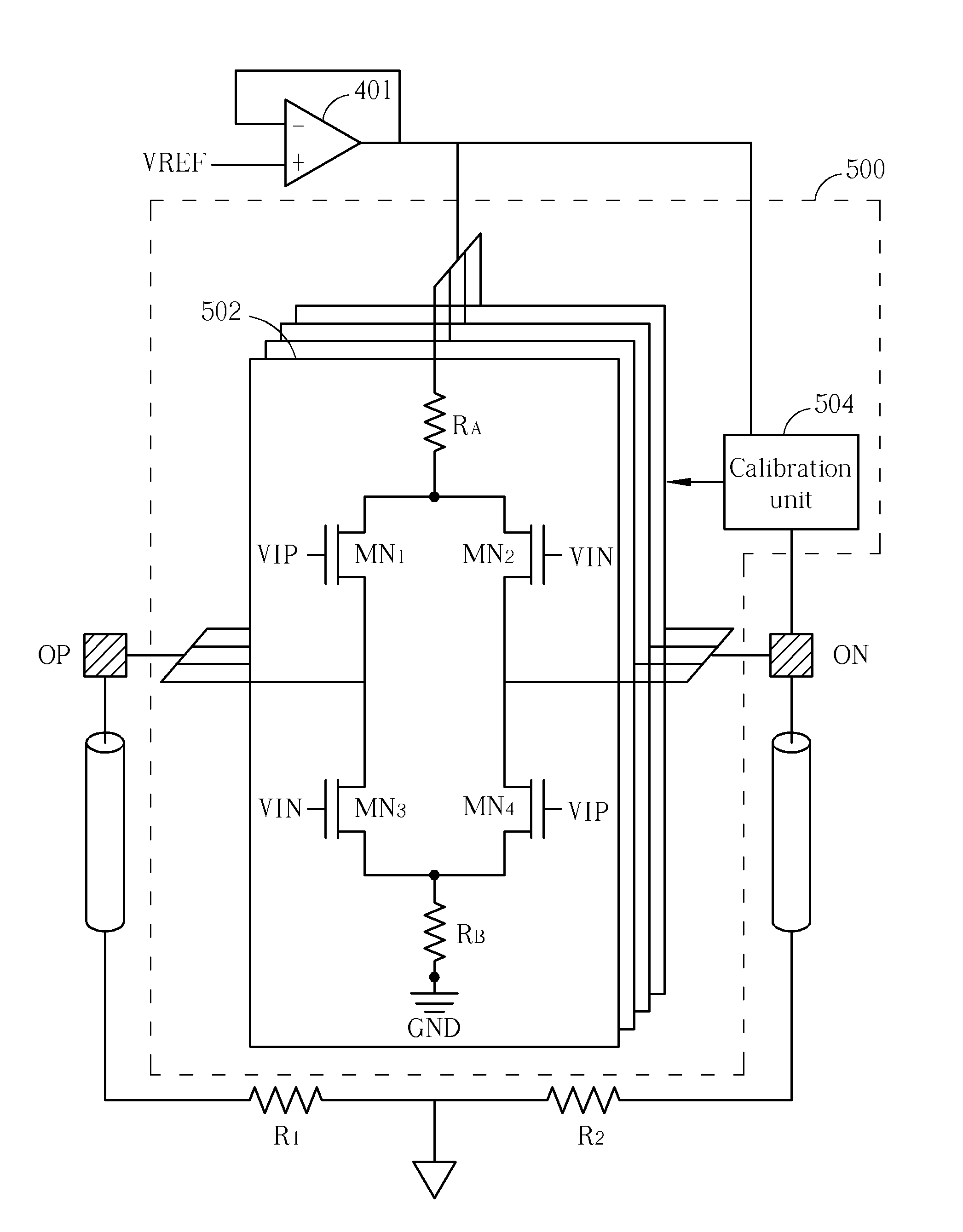
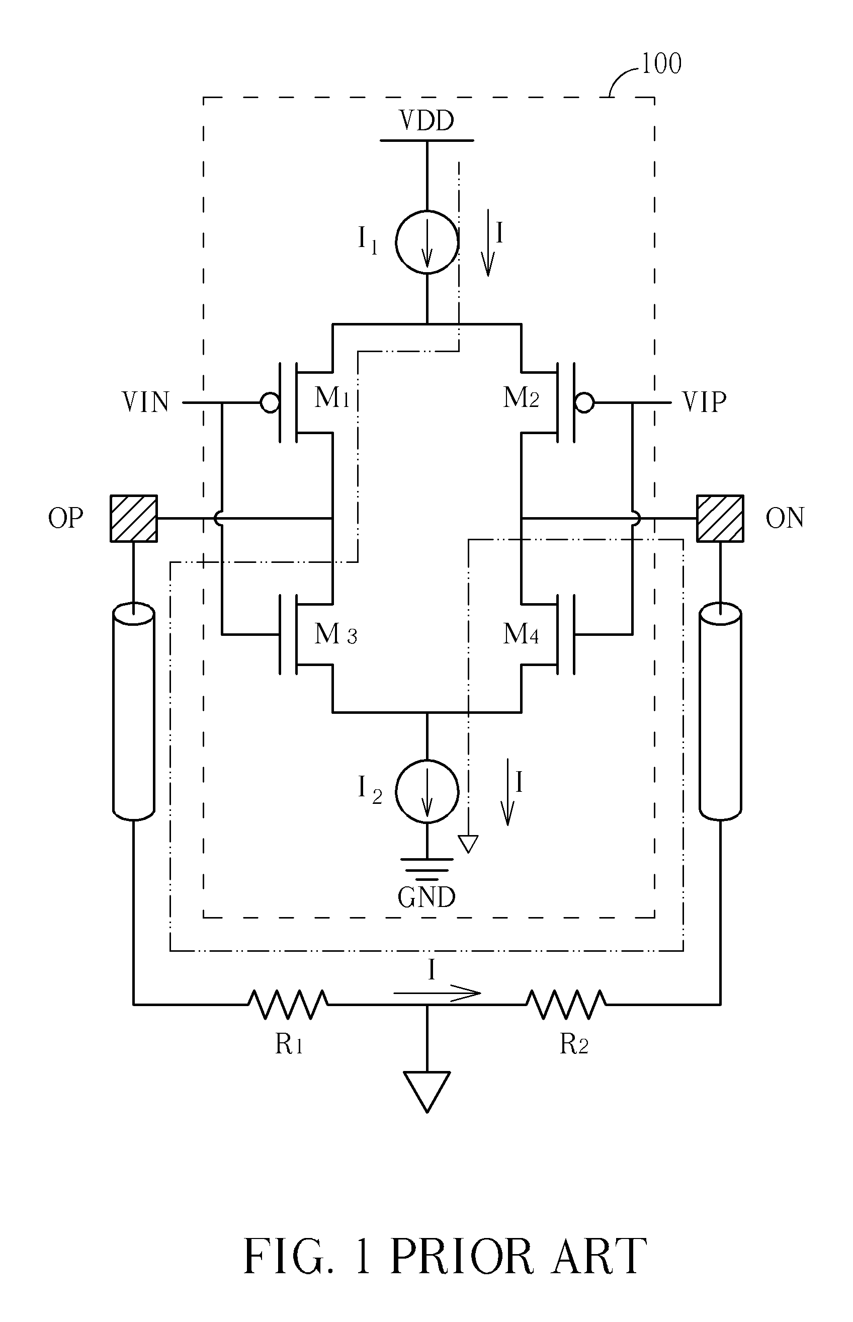
[0016]Please refer to FIG. 4, which shows a driving unit (e.g., an LDVS driver) according to an embodiment of the present invention. The exemplary driving unit 400 includes, but is not limited to, a first bias component RA, a second bias component Re, a first metal-oxide-semiconductor (MOS) transistor MN1, a second MOS transistor MN2, a third MOS transistor MN3, and a fourth MOS transistor MN4, where the first, second, third, and fourth MOS transistors MN1-MN4 have the same conductive type. By way of example, rather than limitation, the first and second bias components RA and RB are implemented using resistors, and the first, second, third, and fourth MOS transistors are N-channel metal-oxide-silicon (NMOS) transistors for a lower threshold voltage. However, this is for illustrative purposes only. Any driving circuit that follows the exemplary circuit architecture shown in FIG. 4 to configure interconnections of implemented bias components and MOS transistors falls within the scope ...


PUM


Abstract

A driving circuit includes at least a driving unit. The driving circuit includes a first bias component, a second bias component, and four metal-oxide-semiconductor (MOS) transistors. The first bias component has a first node coupled to a first reference voltage and a second node for outputting a first bias current. The second bias component has a first node for draining a second bias current and a second node coupled to a second reference voltage different from the first reference voltage. Each of the MOS transistors has a control node for receiving one of input signal pairs, a node coupled to one of the bias components and another node coupled to one of the output ports of the driving circuit. The four MOS transistors are of a same conductive type.

Description

BACKGROUND OF THE INVENTION[0001]1. Field of the Invention[0002]The present invention relates to a driver, and more particularly, to a low power, high speed driving circuit with auto-calibration functionality.[0003]2. Description of the Prior Art[0004]As the resolution of image sensors or display increases, the data rate of becomes very high. As a result, a requirement for a high speed driver with superior performance grows. Among all kinds of high speed drivers, a low voltage differential signal (LVDS) technique is frequently utilized due to a lower electromagnetic interference (EMI), a lower power consumption and a better signal integrity than those of a conventional CMOS full swing driver. Please refer to FIG. 1, which is a diagram of a conventional LVDS driver for driving a pair of loads R1 and R2. The conventional LVDS driver 100 is composed of two PMOS transistors M1, M2, two NMOS transistors M3, M4, and two constant current sources I1 and I2 connected to a reference supply vo...

Claims


Application Information

Patent Timeline
Patent Type & Authority Patents(United States)
IPC IPC(8): H03K19/094
CPCH03K19/018521H03K19/018571H03K19/018585
Inventor LIU, CHIH-MINYIN, PING-HUNG
Owner HIMAX IMAGING LIMITED
Why Eureka
Try Eureka