Methods for forming an RF device with trench under bond pad feature

a technology of rf device and bond pad, which is applied in the direction of semiconductor devices, semiconductor/solid-state device details, electrical apparatus, etc., can solve the problems of degrading device and ic performance, difficult or impossible to provide the desired impedance matching at the input-output terminal of such devices, and achieving convenient planarization polish stop and/or etch stop

Active Publication Date: 2011-08-16
NXP USA INC
View PDF17 Cites 10 Cited by
  • Summary
  • Abstract
  • Description
  • Claims
  • Application Information

AI Technical Summary

Problems solved by technology

Electro-magnetic (E-M) coupling to such low resistivity substrates can make it difficult or impossible to provide the desired impedance matching at the input-output (I / O) terminals of such devices and preserve the desired power output and efficiency.
Further, such E-M coupling can give rise to eddy current losses in the substrate that can further degrade device and IC performance.
These problems become more severe with high periphery devices and higher frequency (e.g., >˜1 GHz) devices since the intrinsic device impedance drops with increasing periphery and increasing frequency, and E-M losses increase as the size of the terminal connections (e.g., the bonding pads) increases.
Unless steps are taken to scale the bonding pad and transmission line impedances at the same time as the intrinsic input-output device impedances scale with frequency and / or power handling capability, overall higher frequency operation and higher power handling capability cannot be reasonably achieved.

Method used


Image

  • Methods for forming an RF device with trench under bond pad feature
  • Methods for forming an RF device with trench under bond pad feature
  • Methods for forming an RF device with trench under bond pad feature

Examples


first embodiment

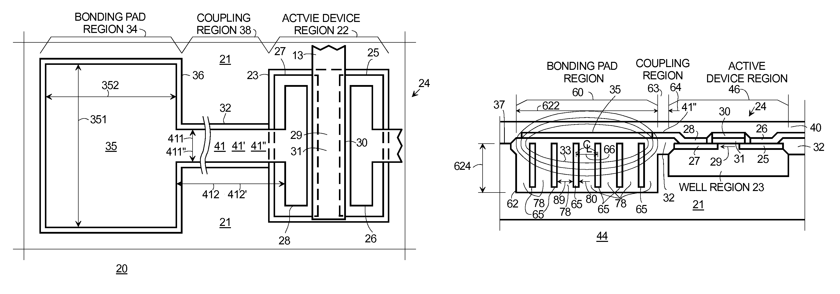
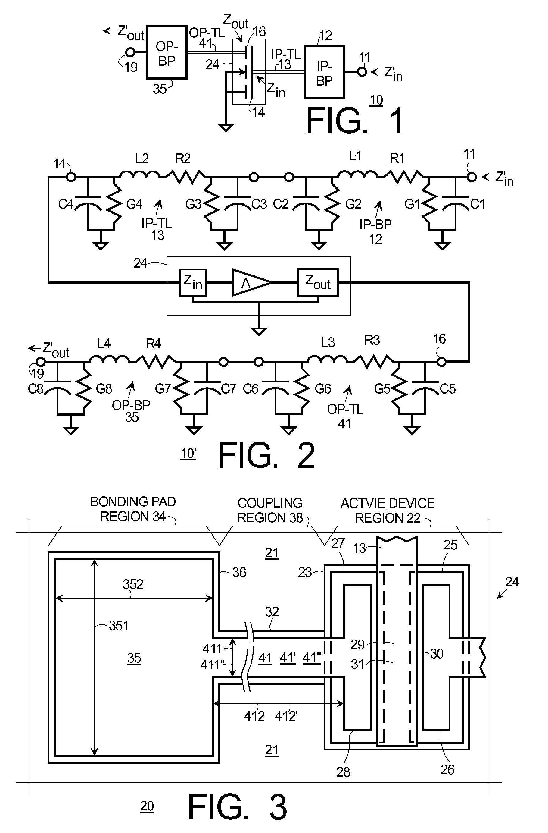
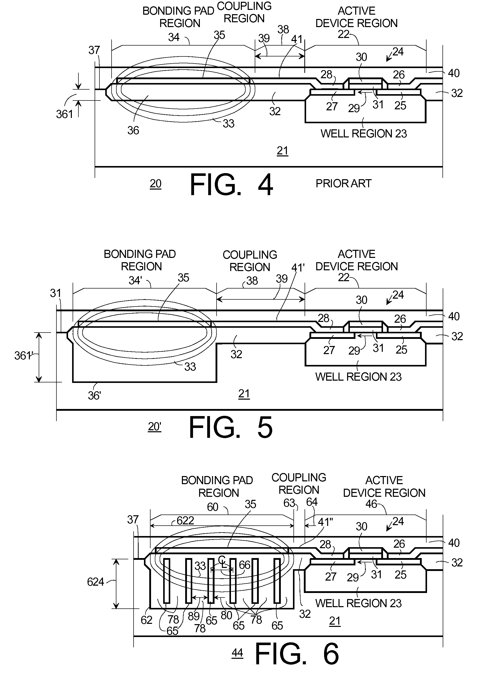
[0046] there is provided an electronic element (44, 44′, 44″), comprising, a semiconductor (SC) substrate (45) having a first thermal expansion coefficient (TEC) and an active device region (46) and a bonding pad region (60), a bonding pad (35) located in the bonding pad region (60), a composite dielectric region (62, 62′, 62″) located in the bonding pad region (60) underlying the bonding pad (35) and comprising an insulating material (78, 78′, 78″) having a second TEC, inclusions (65, 65′, 65″) of a further material (82, 82″; 83, 83″) within the composite dielectric region (62, 62′, 62″), the further material (82, 82″; 83, 83″) having a third TEC less than the second TEC, wherein the inclusions (65, 65′, 65″) are electrically isolated from the substrate (45) and the bonding pad (35), and an active device (24) located in the active device region (46) and proximate the composite dielectric region (62, 62′, 62″), having a first terminal electrically coupled to the bonding pad (35) by ...

second embodiment

[0047] there is provided a method (115-131) for forming an electronic element (44, 44′, 44″) incorporating a composite dielectric region (CDR) (62, 62′, 62″) under a bonding pad (35) coupled to an active device (24), comprising, providing (115, 124, 127) a semiconductor substrate (45) of a first material having a first thermal expansion coefficient (TEC) and having a first surface (57), wherein the substrate (45) has therein a first region (46) adapted to receive the active device (24) and a second region (60) adapted to receive the bonding pad (35), forming (115, 124, 127) a mask (72) on the second region (60), the mask having spaced-apart openings (73, 73′, 73″) of a first width (75, 75′, 75″), etching (116, 124, 127) space-apart trenches (74, 74′, 74″) of substantially the first width (75, 75′, 75″) to a first depth (741, 741″) in the substrate (45), leaving columns (76, 76′, 76″) of substantially undisturbed substrate (45) material between the trenches (74, 74′, 74″) and other p...

third embodiment

[0048] there is provided an electronic device (44, 44′, 44″) comprising, a semiconductor substrate (45) having therein a bonding pad region (60) and an active device region (46), a bonding pad (35) electrically isolated from the substrate (45), a composite dielectric region (62, 62′, 62″) on the substrate (45) in the bonding pad region (60) and underlying the bonding pad (35), wherein the composite dielectric region (62, 62′, 62″) comprises insulating dielectric regions (78, 78′, 78″, 85, 68, 70, 86) and non-single crystal semiconductor inclusion regions (65, 65′, 65″), the inclusion regions (65, 65′, 65″) being electrically isolated from the bonding pad (35) and the substrate (45) by portions of the insulating dielectric regions (78, 78′, 78″, 85, 68, 70, 86), and an active device (24) in the active device region (46) electrically coupled to the bonding pad (35) by an interconnection (41, 41′, 41″). According to a further embodiment, the substrate (45) has a resistivity less than a...


PUM


Abstract

Electronic elements (44, 44′, 44″) having an active device region (46) and bonding pad (BP) region (60) on a common substrate (45) desirably include a dielectric region underlying the BP (35) to reduce the parasitic impedance of the BP (35) and its interconnection (41) as the electronic elements (44, 44′, 44″) are scaled to higher power and / or operating frequency. Mechanical stress created by plain (e.g., oxide only) dielectric regions (36′) can adversely affect performance, manufacturing yield, pad-to-device proximity and occupied area. This can be avoided by providing a composite dielectric region (62, 62′, 62″) having electrically isolated inclusions (65, 65′, 65′) of a thermal expansion coefficient (TEC) less than that of the dielectric material (78, 78′, 78″) in which they are embedded and / or closer to the substrate (45) TEC. For silicon substrates (45), poly or amorphous silicon is suitable for the inclusions (65, 65′, 65″) and silicon oxide for the dielectric material (78, 78′, 78″). The inclusions (65, 65′, 65″) preferably have a blade-like shape separated by and enclosed within the dielectric material (78, 78′, 78″).

Description

FIELD OF THE INVENTION[0001]The present invention generally relates to semiconductor (SC) devices and integrated circuits (ICs) and their methods of manufacture, and more particularly, structures and methods for providing radio frequency (RF) power devices and ICs embodying an insulator filled trench under bond pad feature.BACKGROUND OF THE INVENTION[0002]The performance of radio frequency (RF) power devices and integrated circuits (ICs) is particularly sensitive to the terminal impedances associated with connections to the devices or ICs. This is particularly true for metal-oxide-semiconductor (MOS) field-effect-transistors (MOSFETs) and laterally-diffused-metal-oxide-semiconductor (LDMOS) field effect transistors (FETs) where low resistivity substrates (e.g., <0.1 Ohm-cm) are often used to enhance the active device performance. Electro-magnetic (E-M) coupling to such low resistivity substrates can make it difficult or impossible to provide the desired impedance matching at the ...

Claims


Application Information

Patent Timeline
Patent Type & Authority Patents(United States)
IPC IPC(8): H01L21/44
CPCH01L24/03H01L24/05H01L29/0649H01L2924/13062H01L2924/1306H01L2224/05076H01L2224/05558H01L2924/01002H01L2924/01014H01L2924/01015H01L2924/01027H01L2924/01032H01L2924/01033H01L2924/01057H01L2924/01082H01L2924/05042H01L2924/13091H01L2924/14H01L2924/30105H01L2924/30107H01L2924/3011H01L2924/01006H01L2924/01021H01L2224/05576H01L2924/00H01L2224/023H01L2924/0001
Inventor JONES, JEFFREY K.SZYMANOWSKI, MARGARET A.MIERA, MICHELE L.REN, XIAOWEIBURGER, WAYNE R.BENNETT, MARK A.KERR, COLIN
Owner NXP USA INC
Why Eureka
Try Eureka