RFID tag

a manufacturing method and technology of a rfid tag, applied in the direction of burglar alarm mechanical actuation, burglar alarm by hand-held articles removal, instruments, etc., can solve the problem of difficult formation of fragile parts, easy peeling, weak sticking strength, etc. problem, to achieve the effect of preventing unpredicted antenna peeling and weak sticking strength

Inactive Publication Date: 2011-08-30
HITACHI LTD
View PDF11 Cites 9 Cited by
  • Summary
  • Abstract
  • Description
  • Claims
  • Application Information

AI Technical Summary

Benefits of technology

[0006]Another object of the present invention is to provide a structure which positively cuts off the RFID chip from the antenna as soon as the seal type RFID tag is peeled from the management object in order to make it possible to confirm the removal of the communication function visually as well.
[0015]For forming the sticking layer (the first conductor film) of Ti or Cr and the copper thin film for energization on the main surface of the RFID chip (for example, the wafer), it is desirable to use sputtering or the like. For forming the antenna pattern on the first conductor film or the energization layer (copper thin film) by using plating, it is desirable to use a material having low electrical resistance such as copper or gold. In addition, for removing the sticking layer formed of Ti or Cr from between the antenna pattern formed by plating and the main surface of the RFID chip in a short time, it is desirable to design the antenna pattern so as to accelerate the side etching. For example, if the width of the second part of the antenna (the second conductor film) is made finer than that of the first part (the part for connection to the electrodes for antenna connection), completion of the side etching of the sticking layer is also advanced.
[0017]In the RFID tag according to the second example, the antenna in the RFID chip is formed without forming the sticking layer. After completion of the RFID circuit processes (after completion of the RFID chip), metal which reacts with aluminum easily and which is weak in strength of sticking to the protection film of the RFID chip surface such as gold is vapor-deposited on electrodes for antenna connection (aluminum electrodes) exposed from the main surface of the RFID chip (wafer) and an antenna pattern is formed on the gold film by using a photoresist. Thereafter, the gold film is etched through the photoresist pattern by using an iodine-ammonium iodide solution to shape an antenna. The gold film antenna thus formed is easy to peel from the protection film (insulation film) which covers the main surface of the RFID chip. Therefore, it is desirable to prevent unpredicted antenna peeling by leaving the photoresist material used for etching on the protection film without removing the photoresist material and embedding the photoresist material in the adhesive layer together with the gold antenna in order to avoid peeling of the gold film antenna.
[0018]In the RFID tag according to the present invention, external force applied so as to peel the RFID tag from the adherend extends an adhesive member which fixes the RFID chip to the base member and fixes the RFID tag to the adherend, and peels the antenna on the RFID chip which sticks fast to the adhesive member from the base member to the adherend side. As a result, joining between the antenna and electrodes for antenna connection of the RFID chip is cut off. Therefore, the peeling external force makes it impossible for an external terminal such as a reader or a reader / writer to read the RFID chip. Thus, privacy protection and falsification prevention are achieved.

Problems solved by technology

Since the antenna disposed outside the RFID chip is comparatively large, it can't be denied that there is a possibility that restoration will be able to be conducted by manual work even if connection between the antenna and the RFID chip is destroyed.
On the other hand, the antenna formed on the RFID chip has a firm electrical connection with the RFID chip, and it is difficult to form a fragile part in it.

Method used


Image

  • RFID tag
  • RFID tag
  • RFID tag

Examples


first embodiment

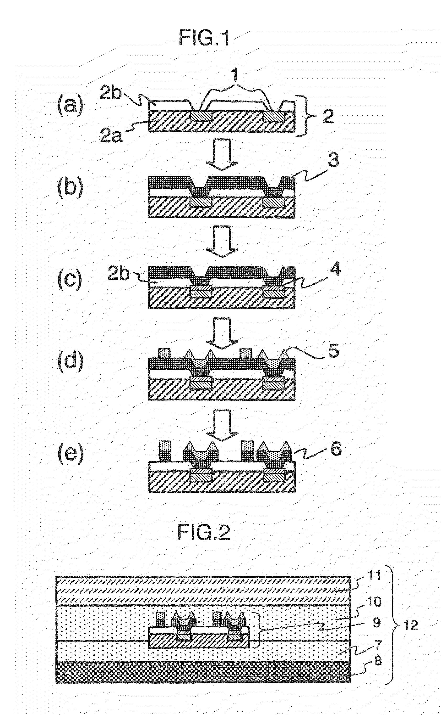
[0030]In the present embodiment, a manufacturing process for forming an RFID tag in which an antenna joined to electrodes formed on a main surface of the RFID chip without a sticking layer, will be described with reference to FIG. 1. In general, the RFID chip (for example, a semiconductor element) is fabricated by using the so-called “wafer unit processing” of forming a plurality of RFID chip circuits on a main surface of a base member (for example, a semiconductor wafer) and then collectively forming antennas on electrodes respectively corresponding to a plurality of RFID chips. A plurality of RFID chips formed in the main surface of the base member are separated into separate RFID chips 9 shown in FIGS. 2 to 4, by cutting the base member. In FIG. 1, the manufacturing process of the RFID chip is shown to be simplified by using a section of an individual piece 2 of a wafer cut out from the base member. However, this illustration does not exclude processing of the photolithographic p...

second embodiment

[0049]In the present embodiment, electrodes (electrodes for antenna connection) formed on the main surface of the RFID chip are connected to an antenna disposed on the main surface with a sticky layer (for example, an additional metal or alloy layer) between.

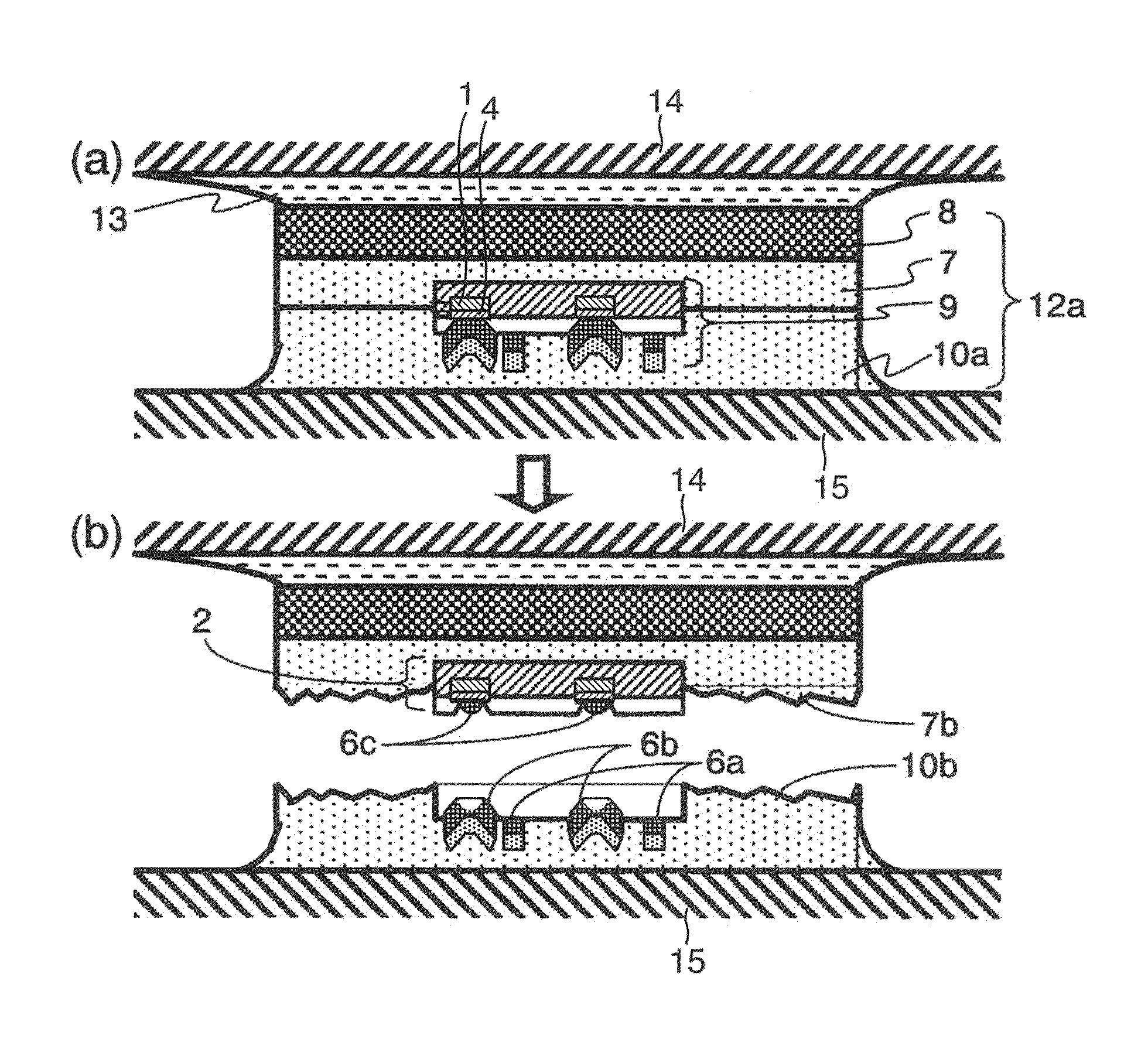
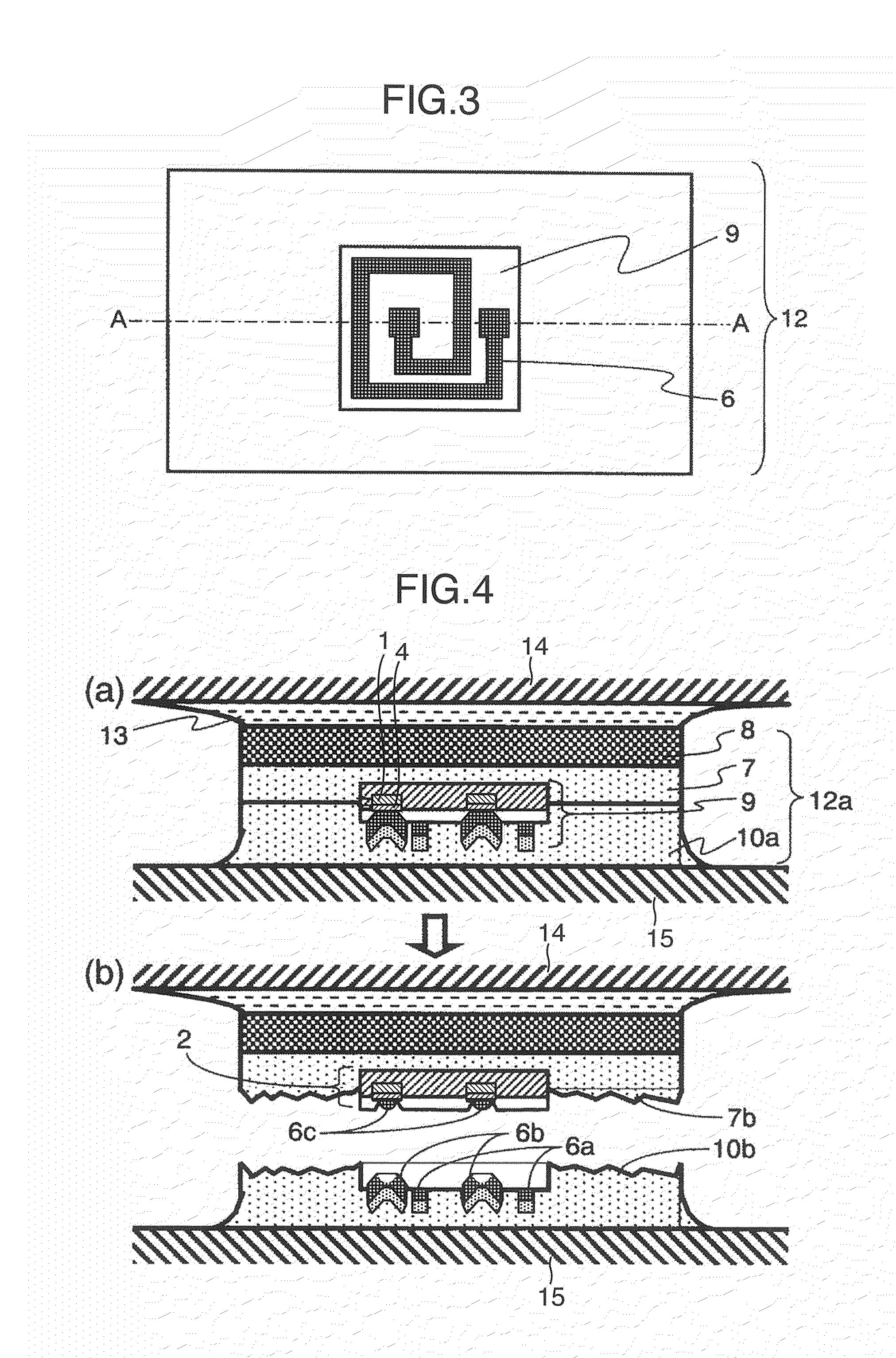
[0050]Manufacturing processes of the RFID chip, a structure of an RFID tag (a seal type RFID chip) on which the RFID chip is mounted, and a form of putting the RFID tag to the adherend will now be described with reference to FIGS. 5 to 7. A section of the RFID chip 900 (wafer 110) shown in FIG. 5 and a section of a seal type RFID tag 1200 having the RFID chip mounted thereon shown in FIG. 6 representing a cross-sectional view taken along an A-A section line drawn in FIG. 7 which shows a plane structure of the seal type RFID tag 1200 together with a perspective image of the main surface of the RFID chip 900 mounted on the RFID tag 1200. Herein, the sticking layer means a body which makes a joining strength of a pair of members jo...

third embodiment

[0060]The RFID tag (12, 1200) described in the first embodiment and the second embodiment exchanges signals (information) with the external terminal by using a loop-shaped or spiral-shaped antenna mounted on the RFID tag. However, the carrier frequency of radio communication using the loop-shaped or spiral-shaped antenna is restricted to the HF band (3 to 30 MHz). If the distance between the RFID tag (12, 1200) and the external terminal is not kept within several cm, signals are not exchanged between them.

[0061]On the other hand, in the RFID tag having a dipole antenna, radio communication with the external terminal can be conducted at a carrier frequency in the UHF band (300 to 3000 MHz). Even if the RFID tag is at a distance of several meters from the external terminal, therefore, signals are exchanged between them.

[0062]As shown in FIG. 8, an RFID tag 12000 according to the present embodiment is formed by mounting an RFID chip 9000 as described in the first embodiment and the sec...


PUM


Abstract

For protecting information stored in an RFID chip and ensuring its authenticity, radio communication between the RFID chip and an external terminal is positively interrupted when a seal type RFID tag including the RFID chip is peeled from an adherend, while ensuring solidity integrity when the RFID tag is put on the adherend. In the seal type RFID tag which includes the RFID chip fixed on a mounting surface of a base member having an adhesive layer applied thereto and which is put on the adherend by using the adhesive layer, an antenna formed on a main surface of the RFID chip is embedded in adhesive layers together with the RFID chip and an adhesive bonding strength between the antenna and the adhesive layer is made greater than a joining strength between the antenna and the RFID chip.

Description

INCORPORATION BY REFERENCE[0001]The present application claims priority from Japanese application JP2007-265071 filed on Oct. 11, 2007, the content of which is hereby incorporated by reference into this application.BACKGROUND OF THE INVENTION[0002]The present invention relates to a structure and a manufacturing method of an RFID tag (especially a tag called seal type RFID tag). In particular, the present invention relates to a technique suitable for preventing information stored in an RFID tag which has become unnecessary for management of an adherend from being read out by an external device (i.e., privacy protection) and ensuring that the RFID is not peeled from the load or product adherend (genuineness or authenticity of the RFID) to which it is attached by making the RFID tag unfunctional when a seal is peeled from the adherend.[0003]An RFID tag (Radio Frequency IDentification-tag) which represents a radio IC tag (non-contact type storage chip tag) designed to have a storage med...

Claims


Application Information

Patent Timeline
Patent Type & Authority Patents(United States)
IPC IPC(8): G08B13/14
CPCG06K19/07749G06K19/07775G06K19/07779G06K19/07798
Inventor KANDA, NAOYAOROKU, NORIYUKI
Owner HITACHI LTD
Why Eureka
Try Eureka