Method of reading the memory plane of a contactless tag

a contactless tag and memory plane technology, applied in the field of methods, can solve the problems of time-consuming and systematic sending of commands to read blocks com_addres, and increase the risk of transmission error

Active Publication Date: 2011-09-27
STMICROELECTRONICS SRL
View PDF8 Cites 2 Cited by
  • Summary
  • Abstract
  • Description
  • Claims
  • Application Information

AI Technical Summary

Benefits of technology

[0017]To address the above-discussed deficiencies of the prior art, an object of the present invention is to propose a reading protocol for accelerating the total or partial reading of the memory plane (or memory dump) without increasing the transmission risk.
[0022]Thus the read command is sent only once, and is replaced for the reading of the following memory words by the sending of an incrementation marker. Such a marker can in practice be limited to a reduced number of bits, for example four. Its transmission at 26.48 kbits / s lasts around 0.15 ms, this being substantially less than the duration of transmission of a block read message. Nevertheless, the reading protocol remains a blockwise reading protocol, thus limiting the size of the transmissions, and hence the attached risks of transmission error.

Problems solved by technology

Now, the larger the size of the memory plane, the larger the risk of transmission error.
Should there be a transmission error with regard to the frame, it is the entire frame that has to be retransmitted.
Having regard to the memory sizes envisaged today for contactless tags, this sequential reading (blockwise) may give rise to a very long time for reading the entire memory plane.
It is in particular the systematic sending of a command to read a block COM_ADDRES that is time-consuming.

Method used


Image

  • Method of reading the memory plane of a contactless tag
  • Method of reading the memory plane of a contactless tag
  • Method of reading the memory plane of a contactless tag

Examples


Embodiment Construction

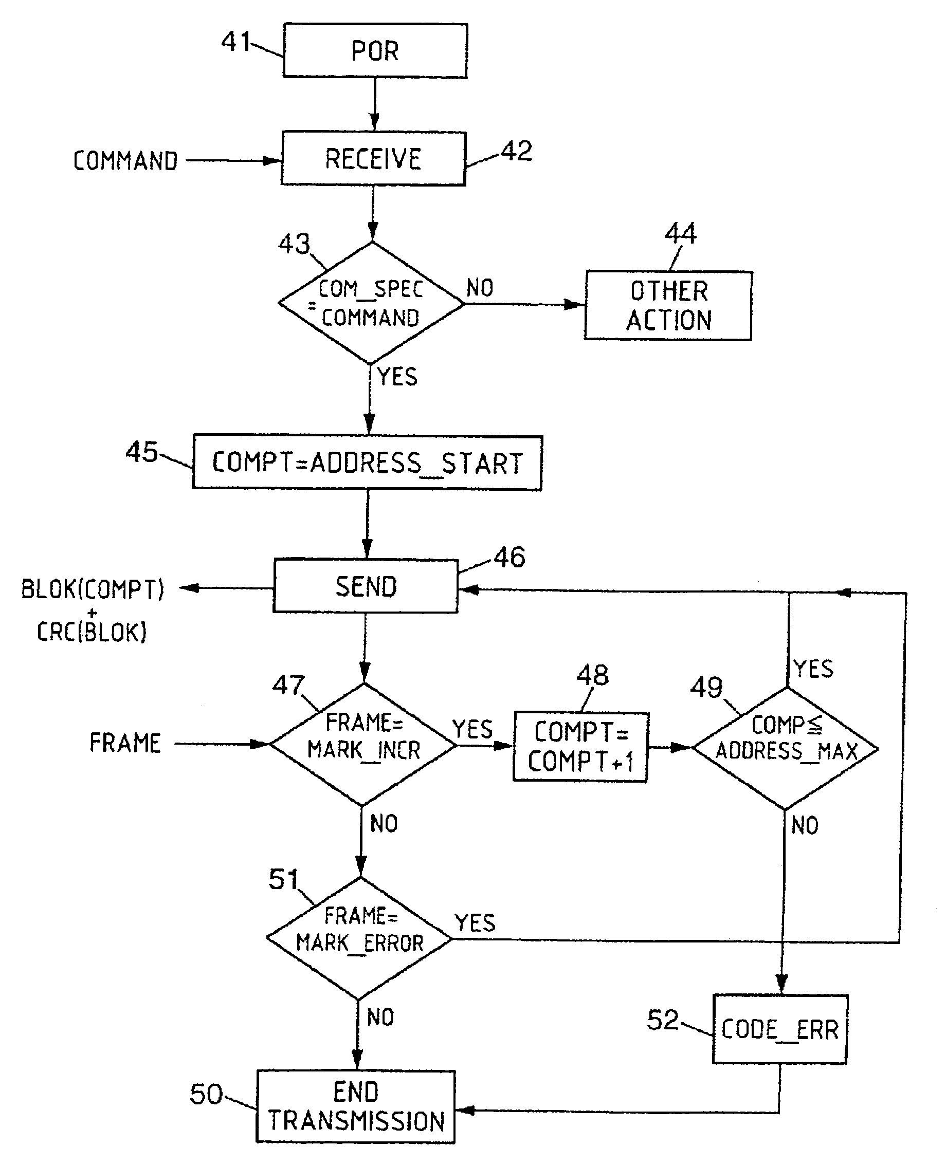
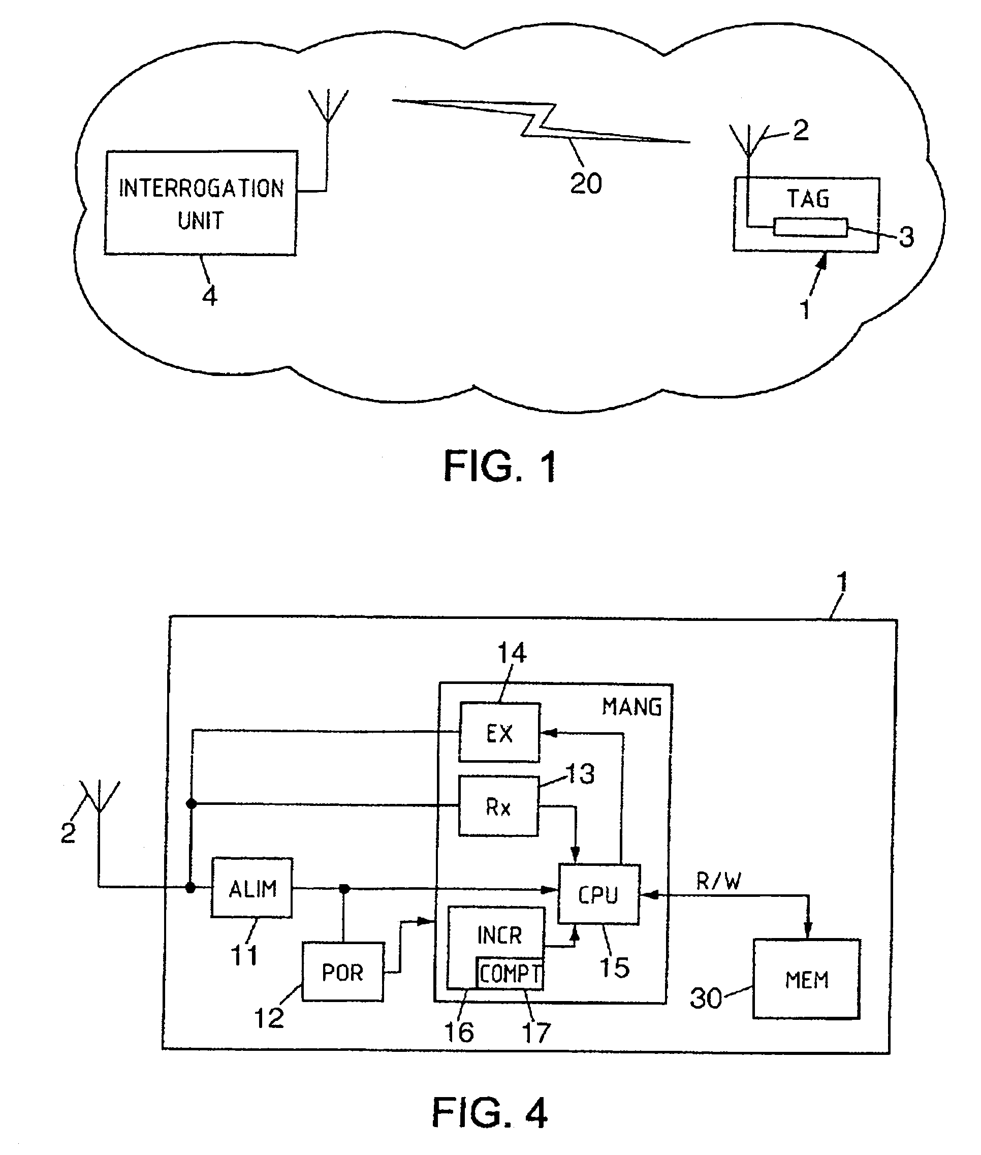
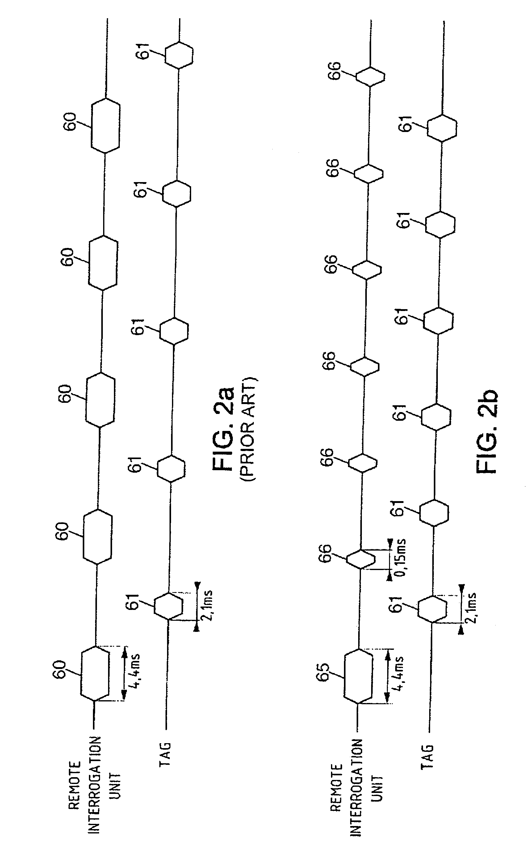
[0037]FIG. 1 has already formed the subject of a description in the above introduction. FIGS. 2b through 4, discussed below, and the various embodiments used to describe the principles of the present invention in this patent document are by way of illustration only and should not be construed in any way to limit the scope of the invention. Those skilled in the art will understand that the principles of the present invention may be implemented in any suitably arranged memory of a contactless tag of RFID type.

[0038]In a general manner, the commands, also called requests, sent by the remote interrogation unit, or the responses transmitted by the contactless tag, are coded and sent in the form of frames of a certain number of bits. The frames for the transmission of commands of a block, for example, are standardized according to the ISO / IEC 15693 standard. The frame structure is of the type:

[0039]

SOFflagsOP CodeidentifieraddressCRCEOF

where:

[0040]“SOF” is a start of frame delimiter field...


PUM


Abstract

A method of reading a group of memory words from an integrated circuit memory of a contactless tag, comprising the sending by a remote interrogation unit to the contactless tag of a specific command for reading the group of memory words from a given start address, the initialization of an address counter for the contactless tag to the value of the given start address, and the sending by the contactless tag of the memory word at the start address, as well as an iterative process comprising in succession a first step of sending by the remote interrogation unit to the contactless tag of an incrementation marker recognizable by the contactless tag, a second step of incrementation of the address counter for the contactless tag in response to the incrementation marker, and a third step of sending by the contactless tag to the remote interrogation unit of a data frame comprising the memory word stored in the memory at the address pointed at by the current value of the address counter.

Description

TECHNICAL FIELD OF THE INVENTION[0001]The present invention relates in a general manner to the reading of data from a memory of a contactless tag of RFID type (standing for “Radio Frequency Identification”). More particularly, it proposes a command allowing accelerated reading, total or partial, of the content of the memory.BACKGROUND OF THE INVENTION[0002]RFID tags, or contactless tags, are being used ever more in everyday life, in particular for the traceability of a range of products, or of products individually. An exemplary RFID tag is presented in FIG. 1. With no energy source of its own, it comprises an antenna 2 and an electronic circuit 3 including a memory in which may be stored various items of information specific to the use of the tag, for example an identification code or (identifier) identifying the tag in particular. An RFID tag is a transmitter / receiver remotely energized by a radio field produced by a remote interrogation unit 4. The tag sends the information store...

Claims


Application Information

Patent Timeline
Patent Type & Authority Patents(United States)
IPC IPC(8): G06F12/00G06F13/28H04Q5/22G06F13/00G06K7/00
CPCG06K7/0008
Inventor MOREAUX, CHRISTOPHERIZZO, PIERRE
Owner STMICROELECTRONICS SRL
Why Eureka
Try Eureka