

Gate valve cleaning method and substrate processing system
a technology of substrate processing and cleaning method, which is applied in the direction of cleaning process and apparatus, cleaning using liquids, cleaning apparatus and processes, etc., can solve the problems of significant reduction of the throughput of the substrate processing system, and achieve the effect of reducing the throughput of the substrate processing apparatus
- Summary
- Abstract
- Description
- Claims
- Application Information
AI Technical Summary
Benefits of technology
Problems solved by technology
Method used
Image

Examples
first embodiment
[0061]First, a description will be given of a substrate processing system according to the present invention.
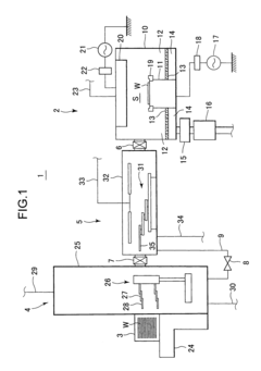
[0062]FIG. 1 is a sectional view schematically showing the construction of the substrate processing system according to the first embodiment.
[0063]As shown in FIG. 1, the substrate processing system 1 is comprised of a process module 2 that subjects semiconductor wafers (hereinafter referred to merely as “wafers”) W as substrates to various plasma processing such as deposition, diffusion, and etching, a loader module 4 that removes each wafer W from a wafer cassette 3 housing a predetermined number of wafers W, and a load-lock module 5 that is disposed between the loader module 4 and the process module 2 and is for transferring each wafer W from the loader module 4 into the process module 2 and from the process module 2 into the loader module 4.
[0064]Each of the process module 2 and the load-lock module 5 is constructed such that the interior thereof can be evacuated, while t...
second embodiment
[0087]Next, a description will be given of a substrate processing system according to the present invention.
[0088]The present embodiment is basically the same as the first embodiment described above in terms of construction and operation, differing from the first embodiment in the construction of the gate valve disposed between the loader module and the load-lock module. Thus, features of the construction and operation that are the same as in the first embodiment will not be described, only features different from those of the first embodiment being described below.
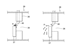
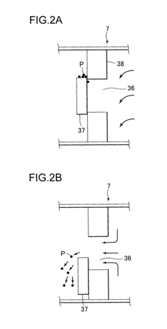
[0089]As shown in FIG. 3A, a gate valve 39 that is disposed between the loader module 4 and the load-lock module 5 and brings them into communication with each other or shuts them off from each other has a nozzle 40 (jetting mechanism) penetrating from outside through the member 38 that defines the wafer transfer port 36 and having a distal end thereof projecting out into the wafer transfer port 36 and bending toward the ...
PUM
 Abstract
Description
Claims
Application Information