Linear image sensor

a line-sequenced image and sensor technology, applied in the field of line-sequenced image sensors, can solve the problems of color data being affected, and achieve the effect of reducing line spacing and high power consumption of comparative color linear image sensors

Inactive Publication Date: 2011-11-15
RENESAS ELECTRONICS CORP
View PDF11 Cites 2 Cited by
  • Summary
  • Abstract
  • Description
  • Claims
  • Application Information

AI Technical Summary

Benefits of technology

[0013]A linear image sensor with a small distance between two photocell arrays (hereafter called “line spacing L1”) is disclosed (See FIG. 1 in Patent Document 1) to decrease the memory capacity to store scanned data and avoid the mechanical misalignment between the photocell arrays. Each element of the linear image sensor is described in the following.
[0020]In the central GR linear image sensor, a photocell array 101b is placed between analog shift registers 102b1 and 102b2. In the RE linear image sensor, analog shift registers are at one side of the color linear image sensor. In the BL linear image sensor, analog shift registers are at another side of the color linear image sensor. Since the arrangement of the photocell array and the analog shift registers for the central linear image sensor is different from those for the outside linear image sensors, both the line spacing L1 between the photocell arrays 101a and 101b and the line spacing L1 between the photocell arrays 101b and 101c can be reduced.
[0027]Since the charge detector is shared between the high and low resolution analog shift registers, the number of output amplifiers can be reduced from two to one per photocell array. Therefore, the power consumption of the linear image sensor can be decreased.
[0029]In the high resolution mode, only the first analog shift register is driven while the second analog shift register is not driven. On the contrary, in the low resolution mode, only the second analog shift register is driven while the first analog shift register is not driven. In this way, coupling noise at the charge detector can be reduced.

Problems solved by technology

If the distance between the two photocell arrays (hereafter called “line spacing”) is wide, a large-capacity external memory is required to store the color data and the color data tends to be affected by the mechanical misalignment of the photocell arrays.

Method used


Image

  • Linear image sensor
  • Linear image sensor
  • Linear image sensor

Examples


example 1

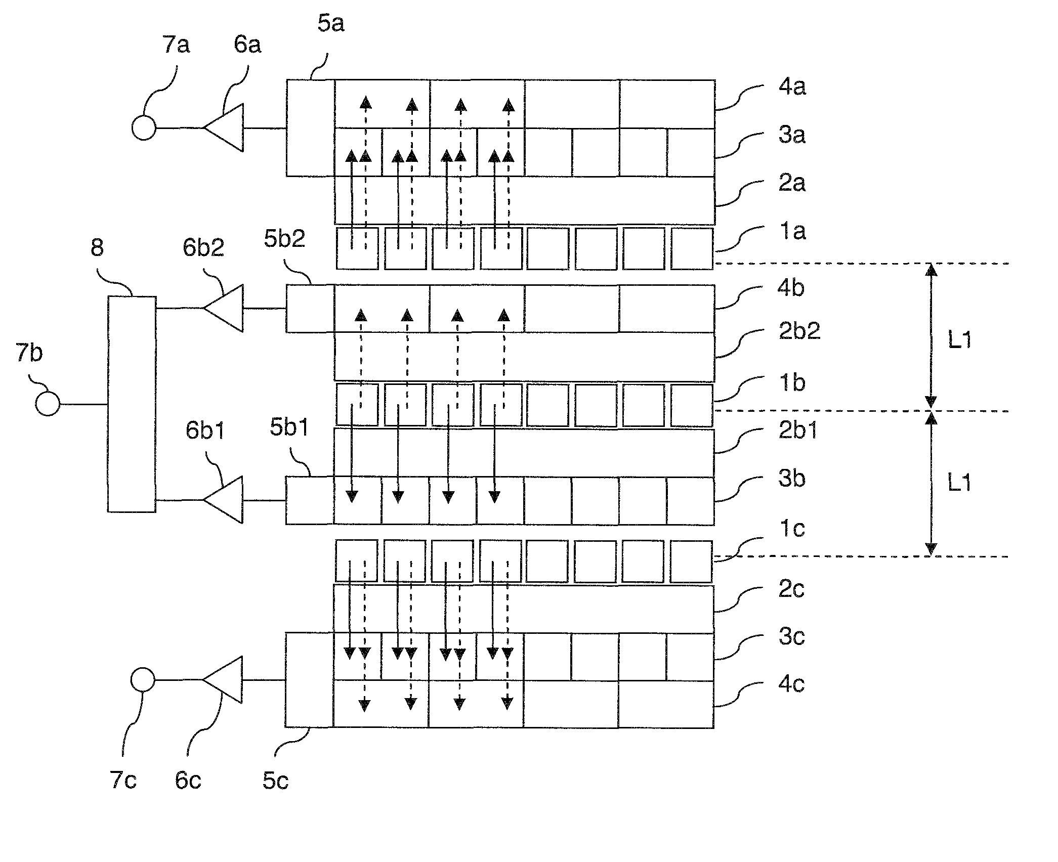
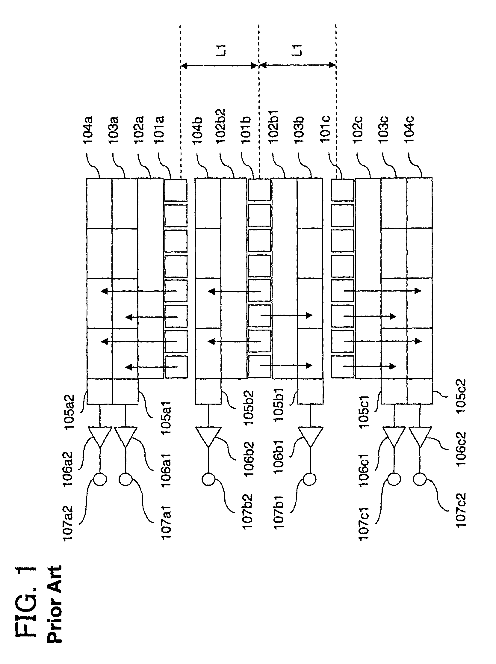
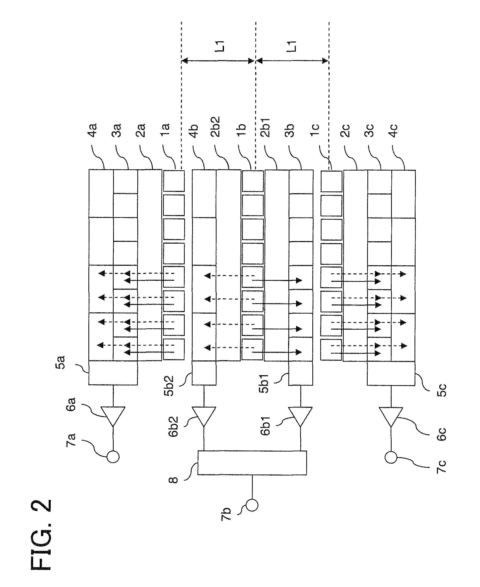
[0048]FIG. 2 shows a linear image sensor according to an example of the present invention. Each component of the image sensor is explained in the following.

[0049]Each photocell array 1a, 1b, 1c is a photodetector to convert incident photons into electrons. The number of photocells determines the resolution in the main scan direction. Here, 1a, 1b and 1c denote a red photocell array, a green photocell array, and a blue photocell array respectively.

[0050]Each transfer gate 2a, 2b1, 2b2 or 2c transfers electrons converted from photons in each photocell to one of analog shift registers.

[0051]The number of stages in each first analog shift register 3a, 3b, 3c used in the high resolution mode is same with the number of photocells in the photocell array.

[0052]The number of photocells in each second analog shift register 4a, 4b, 4c used in the low resolution mode is half the number of photocells in the photocell array.

[0053]A charge detector 5a receives charges from the first and second ana...


PUM


Abstract

A linear image sensor with low noise and low power consumption comprises both high and low resolution analog shift registers for each photocell array. Noise in the output signals is decreased by driving either the low resolution analog shift register or the high resolution analog shift register depending on a required resolution. The power consumption of the linear image sensor is decreased because a charge detector receives charges from the high and low resolution analog shift registers.

Description

RELATED APPLICATION[0001]This application is based upon and claims the benefit of the priority of Japanese patent application No. 2007-004587, filed on Jan. 12, 2007, the disclosure of which is incorporated herein in its entirety by reference thereto.FIELD OF THE INVENTION[0002]The present invention relates to a linear image sensor and more specifically to a linear image sensor with a plurality of analog shift registers.BACKGROUND OF THE INVENTION[0003]There is increasing demand for a color linear image sensor to scan color images because of the recent spread of personal computers and demand for high performance copying machines.[0004]A color linear image sensor usually comprises three linear image sensors disposed in parallel, each having a photocell array to convert received photons into electrons and CCD analog shift registers (hereafter called “analog shift registers”) to transfer the electrons converted from photons in each photocell. Each photocell array is covered with one of...

Claims


Application Information

Patent Timeline
Patent Type & Authority Patents(United States)
IPC IPC(8): H04N9/083H04N3/14H04N5/335H04N9/04H04N1/028
CPCH04N3/1581H04N5/23245H04N5/343H04N5/3452H04N5/3692H04N5/37213H04N23/667H04N25/441H04N25/42H04N25/701H04N25/713
Inventor IKEHATA, YOSHIYUKI
Owner RENESAS ELECTRONICS CORP
Why Eureka
Try Eureka