Antenna device

a technology of an antenna device and an antenna housing, which is applied in the direction of resonant antennas, antenna earthings, elongated active element feeds, etc., can solve the problems of complicated design of the housing of an electronic device, limited permittivity, and difficulty in using patch antennas in wide band communication

Inactive Publication Date: 2011-11-22
SONY CORP
View PDF11 Cites 2 Cited by
  • Summary
  • Abstract
  • Description
  • Claims
  • Application Information

AI Technical Summary

Benefits of technology

[0022]It is further desirable to provide an antenna device of a superior planar structure capable of reducing the area of radiating conductors thereof and exhibiting a wide band characteristic.
[0034]If the antenna device according to the embodiment of the present invention is used to form a wireless communication device, the wireless communication device can be used to perform high-speed and large-volume communication in communication systems of recent years requested to perform wide band communication at a short distance.

Problems solved by technology

However, there is a limitation to the permittivity.
The patch antenna generally tends to operate in a narrow band, and thus is considered to be unsuitable for, for example, a PAN (Personal Area Network) system, the operable band of which is necessary to be wide.
Due to this disadvantage, it is difficult to use the patch antenna in the wide band communication.
In such a case, however, the structure of a housing of an electronic device is complicated in design.

Method used


Image

  • Antenna device
  • Antenna device
  • Antenna device

Examples


Embodiment Construction

[0047]An embodiment of the present invention will be described in detail below with reference to the drawings.

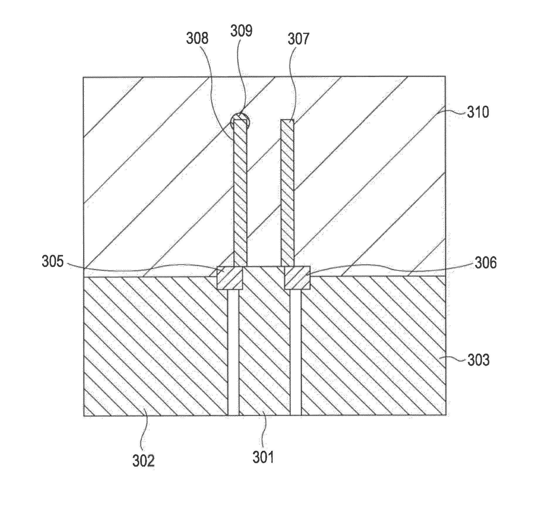
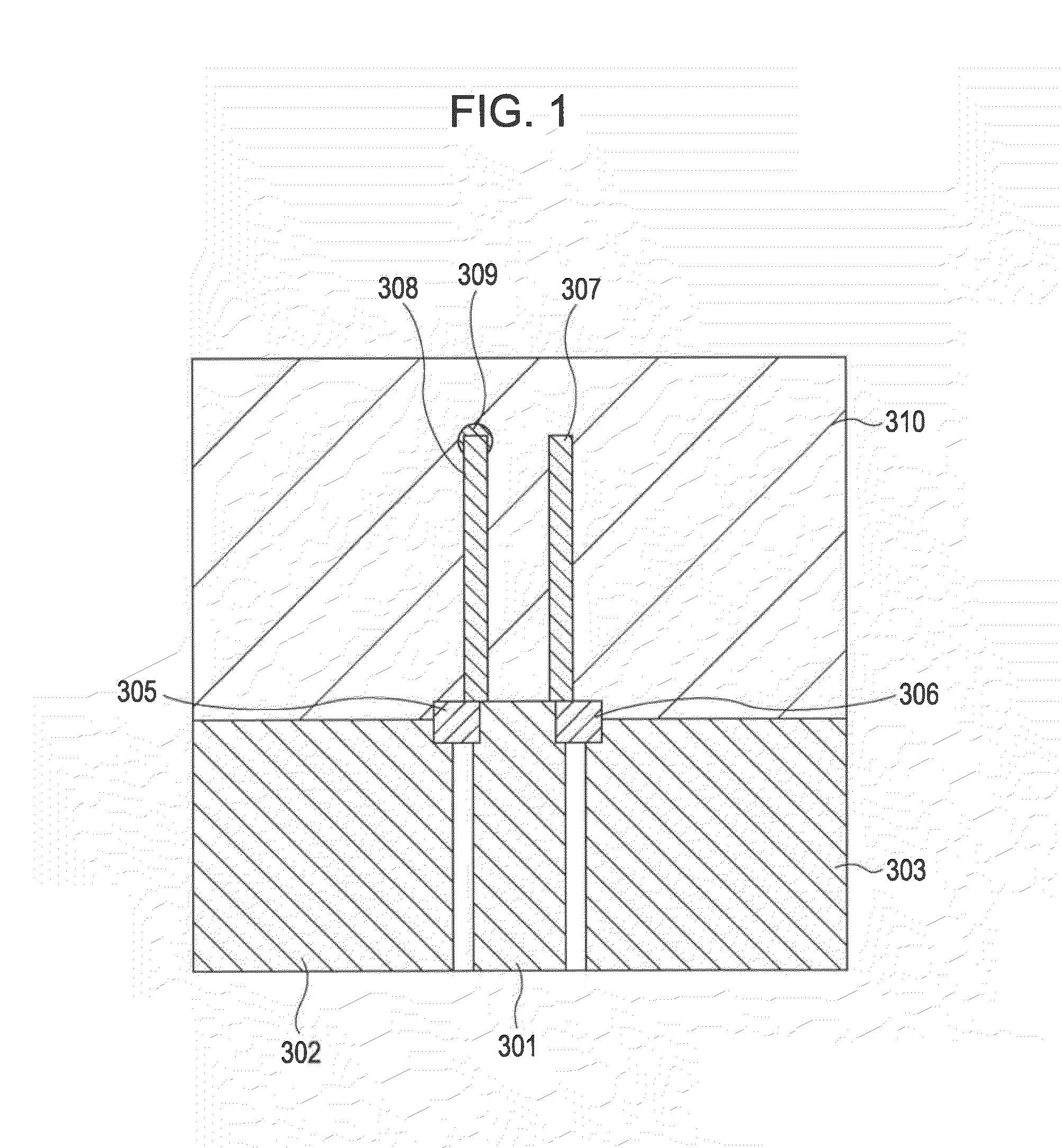
[0048]FIG. 1 illustrates an antenna device according to an embodiment of the present invention, as viewed from above. The antenna device illustrated in the drawing is configured to include two radiating elements 307 and 308, a via hole 309 through which an end of one of the radiating elements 308 is connected to a lower ground (not illustrated), ground conductors 303 and 302 connected to respective base portions of the radiating elements 307 and 308 via resistors 306 and 305, and a feeder line 301 which feeds power to the radiating elements 307 and 308. Similarly to a patch antenna, the antenna device is a planar antenna mountable on a printed board including a thin dielectric layer vertically sandwiched by two conductor layers. The conductor layers include copper or silver, for example, and the dielectric layer 310 includes a glass epoxy resin or Teflon (a registered tradem...


PUM


Abstract

A planar antenna device is mounted on a board including a dielectric layer and two conductor layers vertically sandwiching the dielectric layer. The upper conductor layer includes a first radiating element having an end portion connected through a via hole to a ground formed by the lower conductor layer, a second radiating element having an open end portion, first and second ground conductors connected to respective base portions of the first and second radiating elements via resistors, and a feeder line configured to feed power to the first and second radiating elements.

Description

CROSS REFERENCES TO RELATED APPLICATIONS[0001]The present invention contains subject matter related to Japanese Patent Application JP 2007-319568 filed in the Japanese Patent Office on Dec. 11, 2007, the entire contents of which are incorporated herein by reference.BACKGROUND OF THE INVENTION[0002]1. Field of the Invention[0003]The present invention relates to an antenna device used to transmit and receive a radio signal, and particularly to an antenna device formed by simple combination of planar conductors including a radiating conductor and a ground conductor disposed to face each other with an insulating material interposed therebetween.[0004]More specifically, the present invention relates to an antenna device of a planar structure mountable on a common printed board material or the like of a multilayer structure including layers of a conductor, a dielectric material, and a conductor, for example, and particularly to an antenna device of a planar structure which reduces the are...

Claims


Application Information

Patent Timeline
Patent Type & Authority Patents(United States)
IPC IPC(8): H01Q1/38
CPCH01Q1/38H01Q9/0421H01Q13/08
Inventor YOSHIOKA, MASAHIROKIKUCHI, MASATOMOCHIZUKI, SHUNSUKEARAKI, RYOSUKEHANDA, MASAKINAKANISHI, TAKASHIKIMURA, HIROTOWADA, SEIJIICHIKI, HIROSHIKONDO, TETSUJIRO
Owner SONY CORP
Why Eureka
Try Eureka