Monolithic ceramic electronic component

a technology of electronic components and monolithic ceramics, applied in the direction of fixed capacitor details, capacitors, fixed capacitors, etc., can solve the problems of so-called open mode failure, limit the accuracy of paste coating, and difficulty in accurately forming external terminal electrodes

Active Publication Date: 2011-11-22
MURATA MFG CO LTD
View PDF32 Cites 6 Cited by
  • Summary
  • Abstract
  • Description
  • Claims
  • Application Information

AI Technical Summary

Benefits of technology

To overcome the problems described above, preferred embodiments of the present invention provide a reliable monolithic ceramic electronic component in which waviness of the ceramic green sheets is prevented.
According to preferred embodiments of the present invention, by decreasing the conductor density of the dummy body portion of each of the first and second dummy conductors, ceramic green sheets easily flow toward dummy conductor patterns during stamping which prevents the waviness of the ceramic green sheets. That is, the problem described with reference to FIG. 16 is much less likely to occur. Thus, a reliable monolithic ceramic electronic component can be provided.
In addition, during lamination and sequential pressure-bonding, internal electrode patterns easily flow toward the central portions because of a pressure applied to a portion at which the extended portions of the internal electrodes overlap the dummy body portions of the dummy conductors. Thus, it is possible to further equalize the widths of the exposed ends of the internal electrodes and dummy conductors between one principal surface side and the other principal surface side of the ceramic element assembly. Thus, particularly, when the external terminal electrodes are formed directly by plating, it is possible to form external terminal electrodes having straight edge portions, thus making it possible to prevent that may occur at the time of mounting. That is, the problem described with reference to FIG. 17 and FIG. 18 is much less likely to occur.

Problems solved by technology

If the monolithic ceramic electronic component undergoes such stress, the external terminal electrodes may peel off from the ceramic element assembly to cause a so-called open mode failure.
To prevent such an open mode failure, it is a technical challenge to improve the fixing strength of the external terminal electrodes to the ceramic element assembly.
However, an existing method of baking a thick-film paste limits the accuracy of paste coating, and it is difficult to accurately form the external terminal electrodes.
This may cause a swell (waviness) of the ceramic green sheets in the stamped mother block.
Depending on the situation, there is a possibility that the reliability may decrease because of a structural defect, such as delamination.
This easily causes a swell (waviness) of the ceramic green sheets in the stamped mother block.
This problem is particularly significant when the external terminal electrodes are formed directly by plating.
As described above, when the external terminal electrodes 12 each have a substantially trapezoidal shape, it causes, for example, a tombstone defect or a self-alignment defect due to vertical directivity or increases the likelihood that a solder bridge may occur due to close location of the lower portions of the adjacent substantially trapezoidal shapes.

Method used


Image

  • Monolithic ceramic electronic component
  • Monolithic ceramic electronic component
  • Monolithic ceramic electronic component

Examples


Embodiment Construction

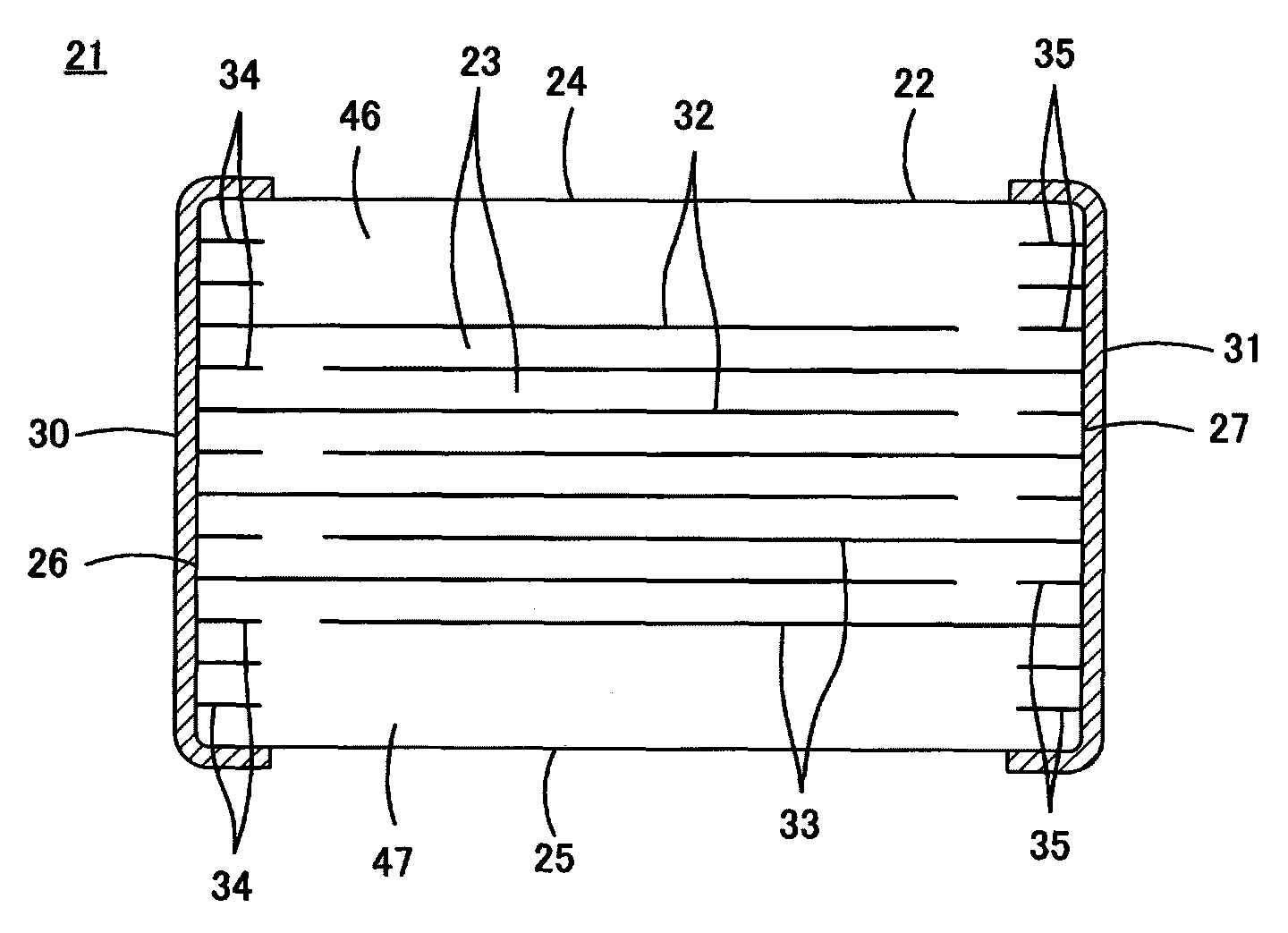
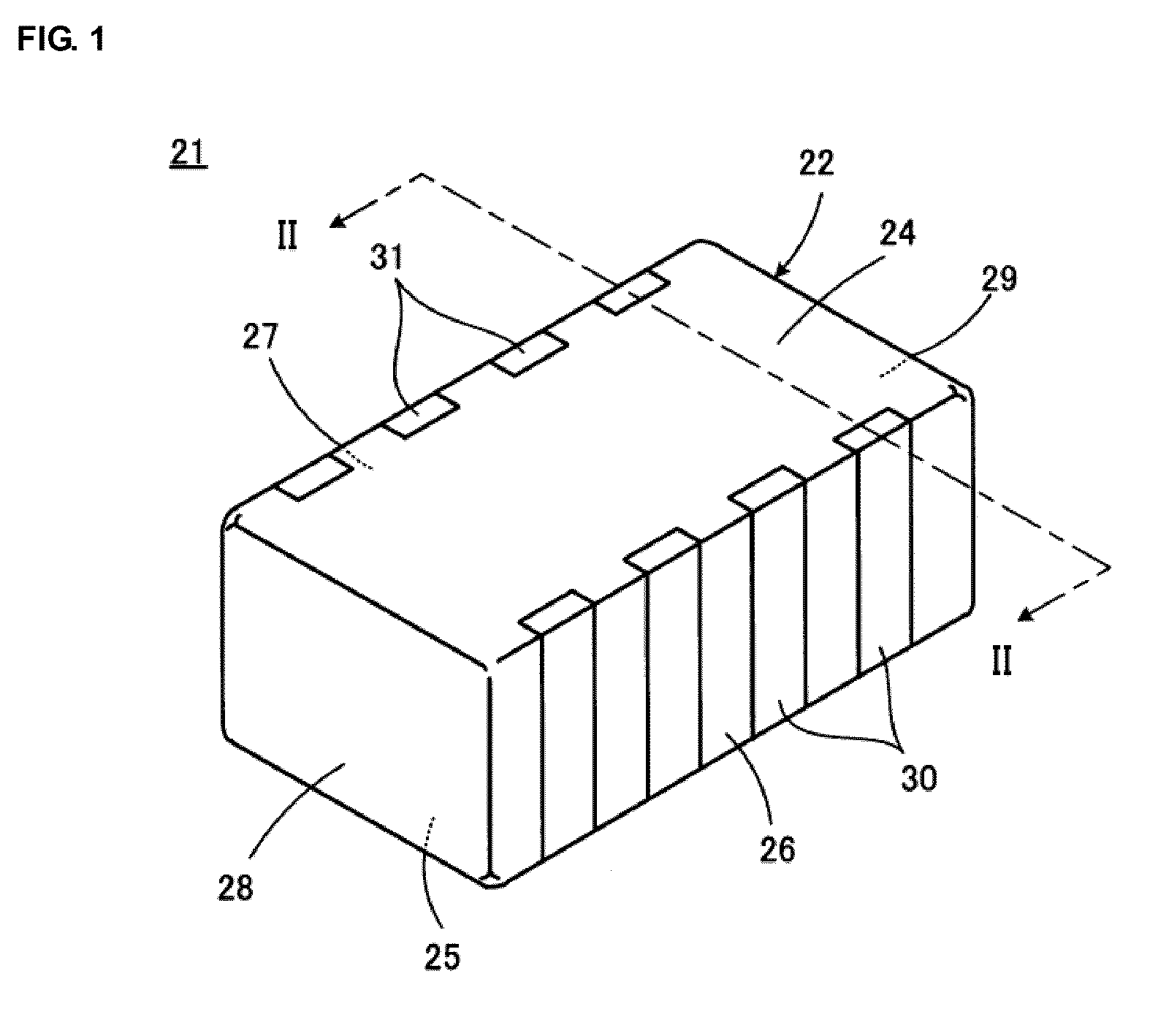
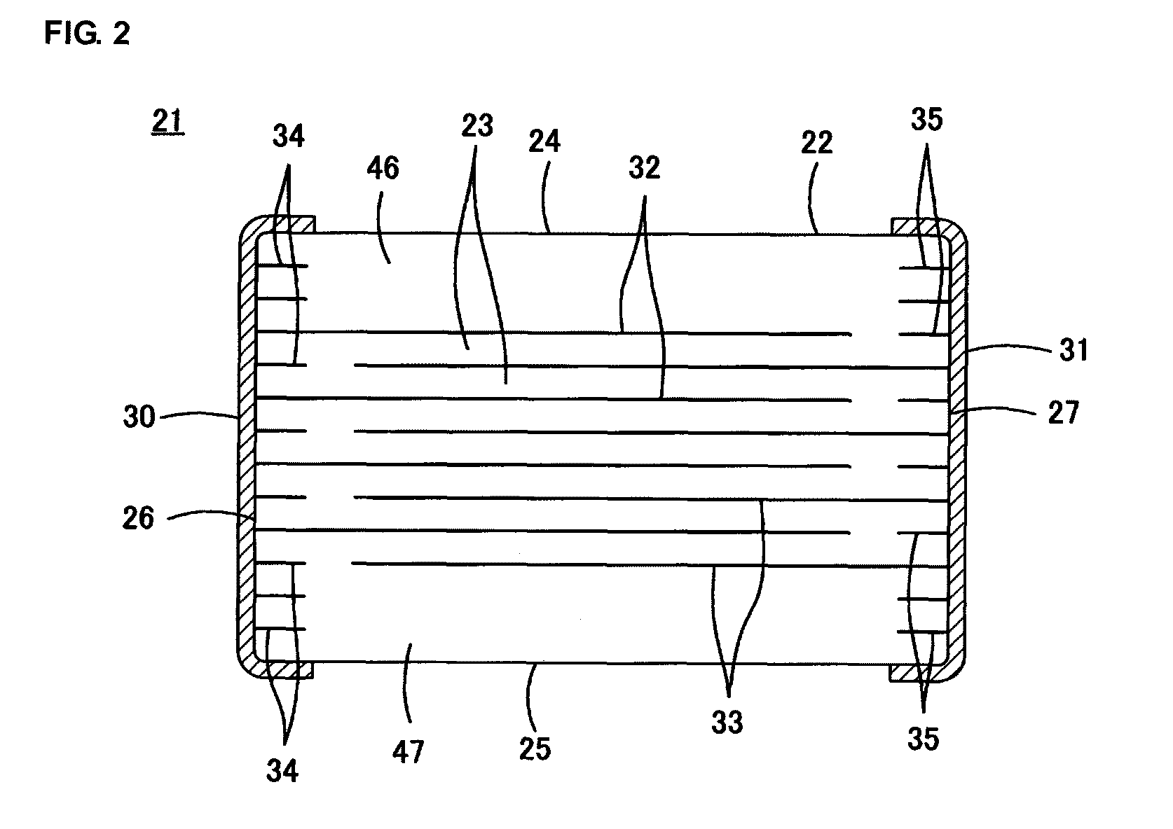
FIG. 1 to FIG. 9 illustrate a monolithic ceramic electronic component 21 according to a first preferred embodiment of the present invention. FIG. 1 is a perspective view showing the monolithic ceramic electronic component 21. FIG. 2 is a cross-sectional view taken along the line II-II in FIG. 1. FIG. 3A to FIG. 3F are plan views showing the internal structure of a ceramic element assembly 22 included in the monolithic ceramic electronic component 21 shown in FIG. 1, and showing typical configurations in cross section.

As shown in FIG. 1 to FIG. 3F, the ceramic element assembly 22 of the monolithic ceramic electronic component 21 includes a plurality of laminated ceramic layers 23. The ceramic element assembly 22 has a first principal surface 24 and a second principal surface 25 that are opposite to each other, and first to fourth side surfaces 26 to 29 that connect the first principal surface 24 with the second principal surface 25. The first side surface 26 and the second side surfa...


PUM

PropertyMeasurementUnit
thicknessaaaaaaaaaa
thicknessaaaaaaaaaa
thicknessaaaaaaaaaa

Abstract

A monolithic ceramic electronic component includes a dummy electrode having a dummy body portion and an internal electrode having an extended portion, in which the conductor density of the dummy body portion is less than the conductor density of the extended portion of an internal electrode. With this configuration, the fixing strength of an external terminal electrode to a ceramic element assembly is improved, and undesirable deformation caused by a dummy conductor provided in a monolithic ceramic electronic component is prevented.

Description

BACKGROUND OF THE PRESENT INVENTION1. Field of the InventionThe present invention relates to a monolithic ceramic electronic component and, more particularly, to a monolithic ceramic electronic component in which an external terminal electrode is not only connected to exposed ends of internal electrodes but also connected to exposed ends of dummy conductors to thereby improve the fixing strength of the external terminal electrode.2. Description of the Related ArtIn recent years, miniaturization of electronic apparatuses, such as a cellular phone, a notebook computer, a digital still camera and a digital audio instrument, has progressed, and these electronic apparatuses use a large number of monolithic ceramic electronic components that enable miniaturization and provide high performance.Generally, each monolithic ceramic electronic component includes a ceramic element assembly, internal electrodes, and external terminal electrodes. The ceramic element assembly includes a plurality o...

Claims


Application Information

Patent Timeline
Patent Type & Authority Patents(United States)
IPC IPC(8): H01G4/30
CPCH01G4/30H01G4/012
Inventor YOSHIDA, AKIHIROMATSUMOTO, HIROYUKI
Owner MURATA MFG CO LTD
Why Eureka
Try Eureka