Reducing stress between a substrate and a projecting electrode on the substrate

a technology of projecting electrodes and substrates, applied in the field of semiconductor components, can solve the problems of silicon breakout, delamination of layers, cracking of isolation layers on substrates, etc., and achieve the effect of improving thermal contact, mechanical connection footprint, and area fraction of the first substrate-face section

Active Publication Date: 2011-12-20
NXP BV
View PDF13 Cites 0 Cited by
  • Summary
  • Abstract
  • Description
  • Claims
  • Application Information

AI Technical Summary

Benefits of technology

[0005]The semiconductor component of the first aspect of the invention reduces the stress exerted from the projecting electrode to the substrate by means of a reduced contact area of mechanical connection between the projecting electrode and the substrate in the second substrate-face section, in comparison with the full area of the substrate face of the projecting electrode. If mechanical stress is exerted, the projecting electrode has the ability to comply to the stress by a deformation of the projecting electrode relative to the substrate in three dimensions. The gap that separates the projecting electrode from the substrate in the first substrate-face section of the substrate face of the projecting electrode reduces the coupling between the projecting electrode and the substrate and enables the deformation of the projecting electrode.
[0038]Preferably, removing the layer from between the recess structure and the substrate-face of the projecting electrode in its first substrate-face section comprises exposing the layer to an etchant. A liquid etchant is preferred. In order to promote the distribution of the liquid etchant in the second substrate-face section, fabricating the recess structure preferably comprises fabricating slits in the recess structure, which slits have a lateral width that promotes the distribution of the liquid etchant by capillary effects.

Problems solved by technology

Such mechanical stress due to a difference in thermal expansion coefficients can produce a crack of an isolation layer on the substrate of the semiconductor component, a delamination of layers, or even a breakout of silicon.

Method used


Image

  • Reducing stress between a substrate and a projecting electrode on the substrate
  • Reducing stress between a substrate and a projecting electrode on the substrate
  • Reducing stress between a substrate and a projecting electrode on the substrate

Examples


Embodiment Construction

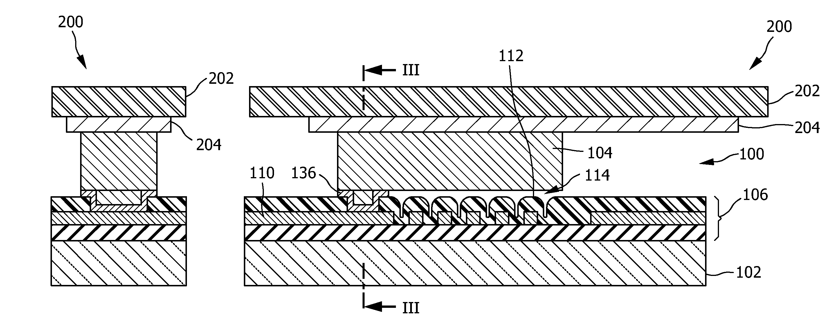
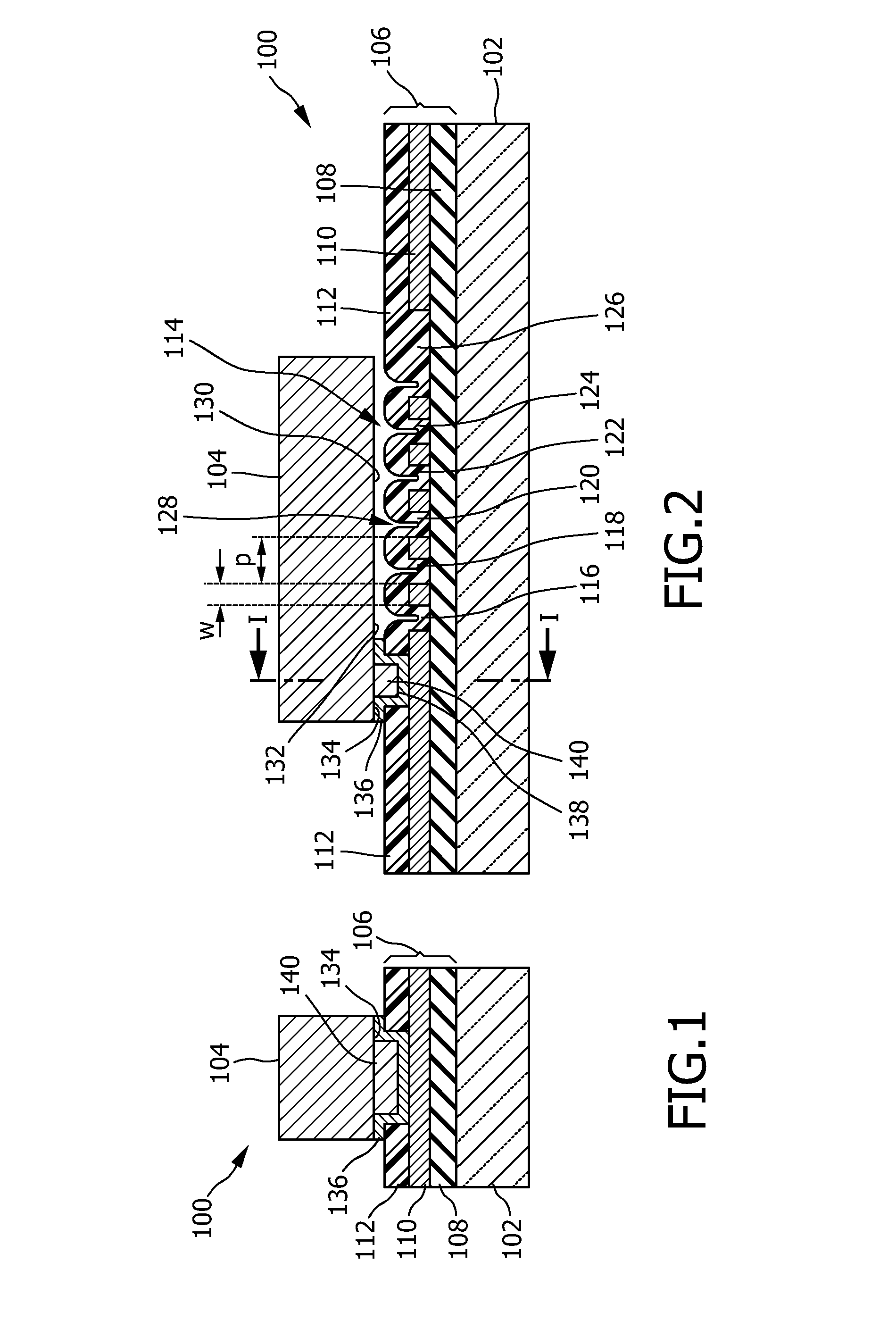
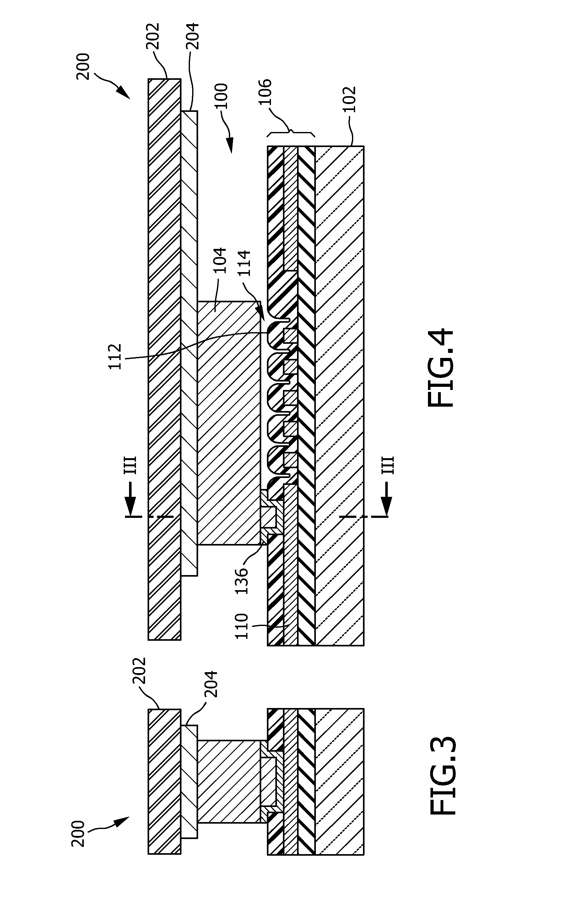
[0049]FIGS. 1 and 2 show schematic cross-sectional views of an embodiment of a semiconductor component. The two cross-sectional views of FIGS. 1 and 2 show sectionals planes, which are perpendicular to each other. The sectional plane shown in FIG. 1 is indicated by a dashed line I-I in FIG. 2. In the following, reference is made to FIGS. 1 and 2 in parallel.

[0050]The semiconductor component 100 has a substrate 102 and a projecting electrode in the form of a bump 104 on the substrate 102. The substrate 102 contains integrated circuits (not shown), and is covered by a layer stack 106, which contains an isolation layer 108, a metallization layer 110, and a passivation layer 112. The passivation layer 112 is made of silicon dioxide or silicon oxynitride or silicon nitride or a combination of these, for instance in the form of a layer structure, such as a sandwich layer structure. Organic materials are also possible, e.g., polyimide. The metallization layer is made of Al with a content o...


PUM


Abstract

The present invention relates to a semiconductor component that has a substrate and a projecting electrode. The projecting electrode has a substrate face, which faces the substrate and which comprises a first substrate-face section separated from the substrate by a gap. The gap allows a stress-compensating deformation of the projecting electrode relative to the substrate. The substrate face of the projecting electrode further comprises a second substrate-face section, which is in fixed mechanical and electrical connection with the substrate. Due to a smaller footprint of mechanical connection between the projecting electrode and the substrate, the projecting electrode can comply in three dimensions to mechanical stress exerted, without passing the same amount of stress on to the substrate, or to an external substrate in an assembly. This results in an improved lifetime of an assembly, in which the semiconductor component is connected to an external substrate by the projecting electrode.

Description

FIELD OF THE INVENTION[0001]The present invention relates to a semiconductor component having a substrate and a projecting electrode on the substrate for electrically connecting the semiconductor component to an external substrate. The present invention further relates to a component-external-substrate assembly, comprising a semiconductor component and an external substrate, to a method for fabricating a semiconductor component, and to a method for fabricating a component-external-substrate assembly.BACKGROUND OF THE INVENTION[0002]For mounting a semiconductor component, such as a chip comprising integrated circuitry, on an external substrate, such as a circuit board, it is a well-known technique to bond the semiconductor component to the external substrate by means of projecting electrodes on an internal substrate of the semiconductor component. The projecting electrodes often take the form of bumps. Note that the internal substrate of the semiconductor component will hereinafter b...

Claims


Application Information

Patent Timeline
Patent Type & Authority Patents(United States)
IPC IPC(8): H01L21/70
CPCH01L24/11H01L24/13H01L24/81H01L2924/1461H01L2224/03912H01L2224/114H01L2224/1147H01L2224/116H01L2224/13099H01L2224/13124H01L2224/13144H01L2224/13147H01L2224/81801H01L2924/01004H01L2924/01013H01L2924/01015H01L2924/01029H01L2924/01032H01L2924/01033H01L2924/01047H01L2924/01074H01L2924/01078H01L2924/01079H01L2924/01082H01L2924/10329H01L2924/14H01L2924/014H01L2224/0401H01L2924/00H01L2224/05124H01L2224/05147H01L24/03H01L24/05H01L2924/00014H01L2924/013H01L2924/01014
Inventor JASPER, JOERGJASPER, LEGAL REPRESENTATIVE, UTE
Owner NXP BV
Why Eureka
Try Eureka