

Method for manufacturing a ferroelectric member element structure
a technology of ferroelectric components and elements, applied in the direction of piezoelectric/electrostrictive transducers, generators/motors, conductive pattern formation, etc., can solve the problems of large stress applied to the interfaces between these layers, the method of manufacturing elements by machining, and the inability to simplify the structure of layers
- Summary
- Abstract
- Description
- Claims
- Application Information
AI Technical Summary
Benefits of technology
Problems solved by technology
Method used
Image

Examples
first embodiment
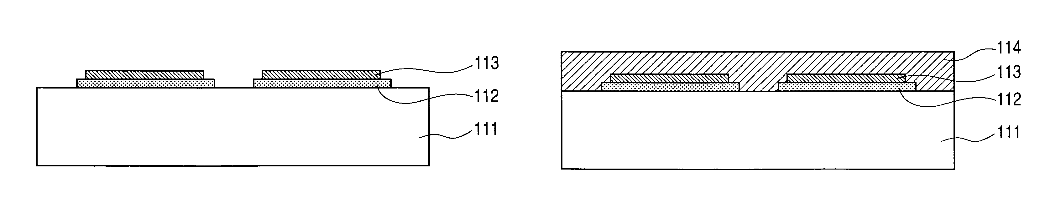
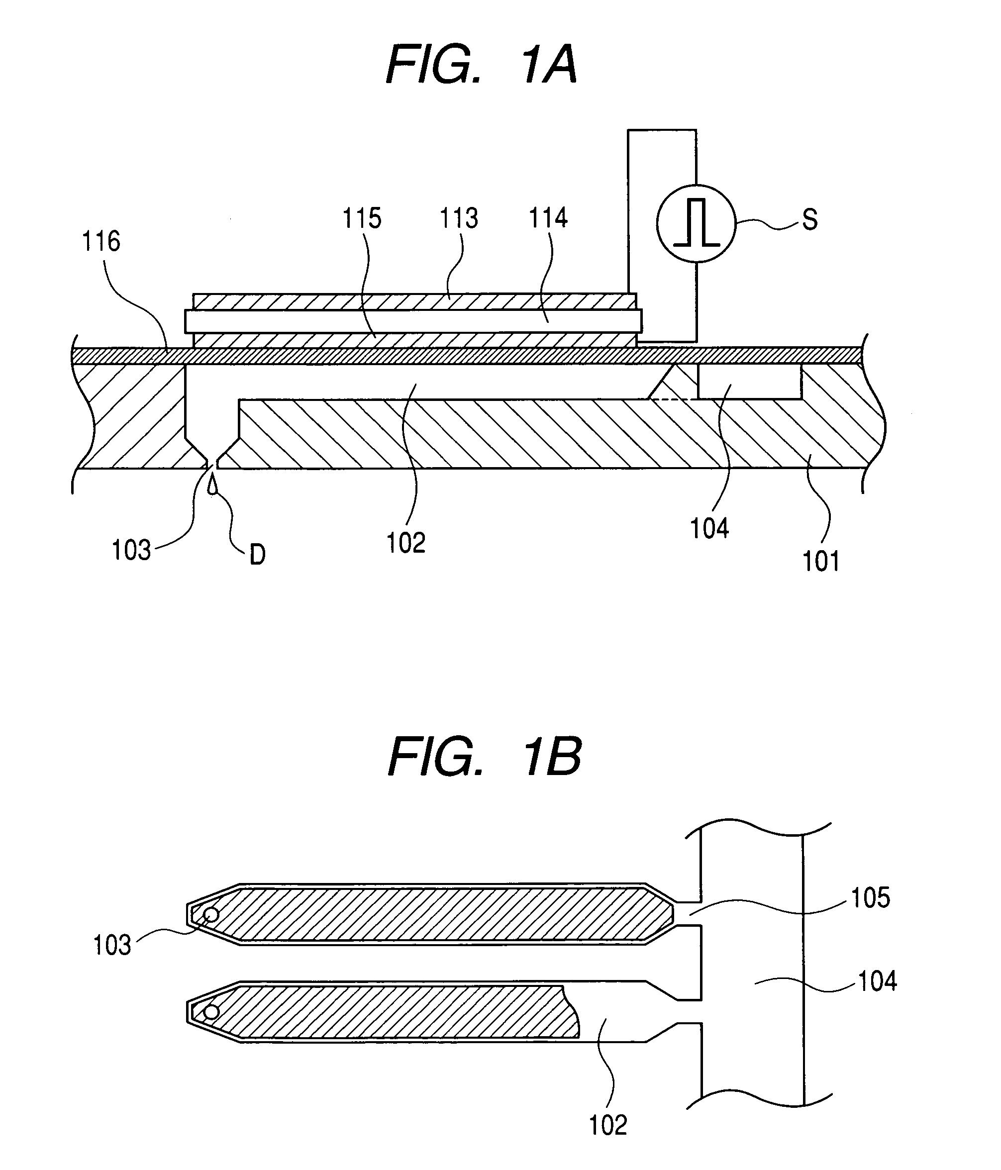
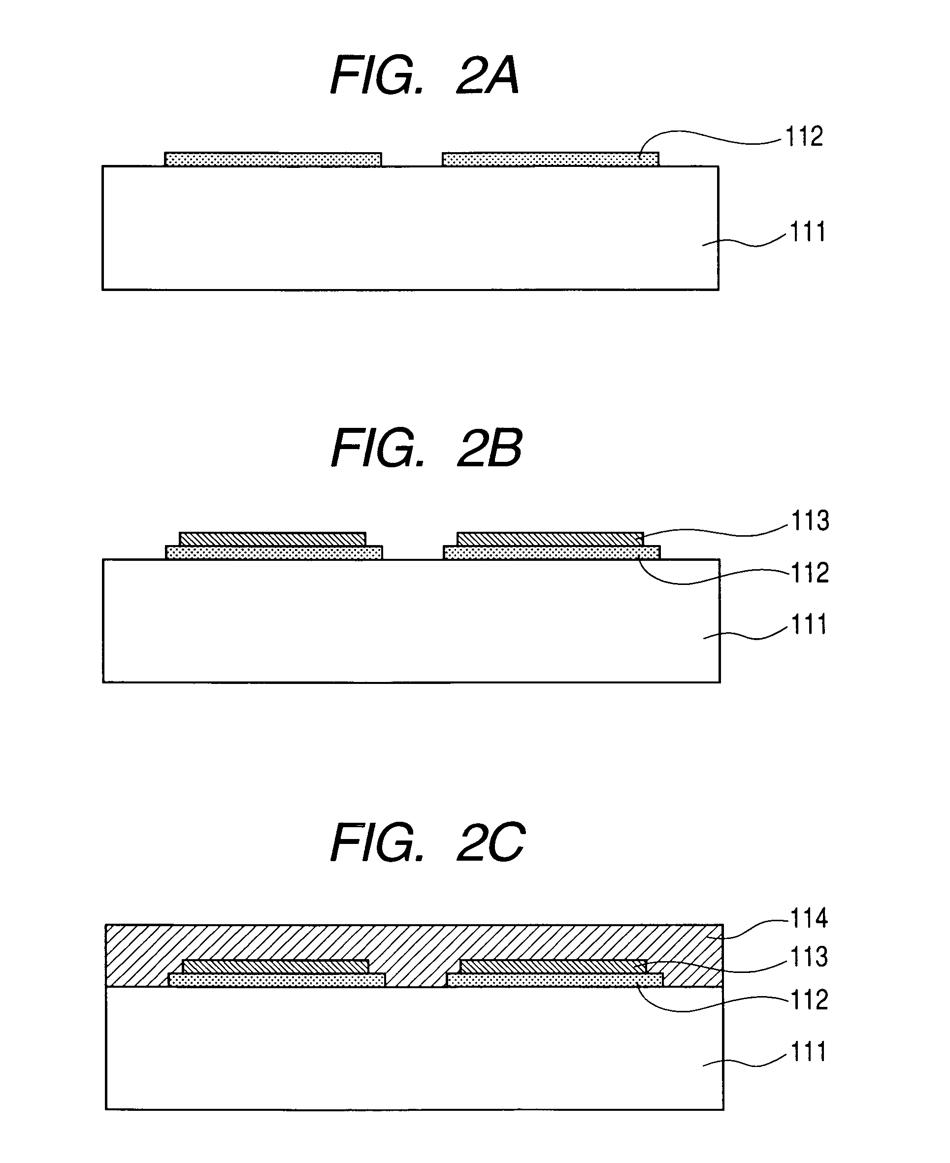
[0093]FIG. 1A is an enlarged sectional view of a printer head using the piezoelectric / electrostrictive element structure according to a first embodiment of the present invention, sectioned in parallel with a longitudinal direction of a vibrating plate 116, and FIG. 1B is a partial enlarged view of the printer head, viewed from the above. In the printer head, a substrate 101 comprised of a silicon substrate having a thickness of 200 μm is subjected to dry etching from upper and lower directions to form a plurality of recessed portions including discharge ports 103 arranged with pitch of 200 dpi, and plural liquid chambers 102 are formed by covering the recessed portions with vibrating plates 116 formed on the piezoelectric / electrostrictive element structure of the present invention, which will be described later, and by joining the vibrating plates 116 to the substrate 101. Each liquid chamber 102 is formed to have a width of 65 μm, a length of 3000 μm and a depth of 100 μm, and long...
second embodiment
[0105]FIG. 9A to FIG. 10C are views for mainly explaining the manufacturing method of a piezoelectric / electrostrictive element structure according to a second embodiment of the present invention in the manufacturing process of the printer head and are sectional views looked at from a direction perpendicular to the arrangement pitch of the discharge ports 103. Here, the construction of the printer head is similar to the first embodiment. The printer head according to this embodiment was manufactured by using SOI-Epi wafer / ELTRAN (manufactured by Canon) 320 having a thickness of about 500 μm. In this ELTRAN, an SiO2 layer 322 and a monocrystal Si layer 323 are formed on an Si layer 321, wherein the Si layer 321 fills the fundamental role of forming respective liquid chambers, the SiO2 layer 322 acts as an etching stopping layer and a vibrating plate and the monocrystal Si layer 323 acts as a monocrystal substrate used in the manufacture of a ferroelectric member structure. The ELTRAN ...
third embodiment
[0110]FIG. 11A to FIG. 12C are views for mainly explaining the manufacturing method of a piezoelectric / electrostrictive element structure according to a third embodiment of the present invention in the manufacturing process of the printer head and are sectional views looked at from a direction perpendicular to the arrangement pitch of the discharge ports. Here, the construction of the printer head is similar to the first embodiment. The printer head according to this embodiment was manufactured by using SOI-Epi wafer / ELTRAN (manufactured by Canon) 420 having a thickness of about 500 μm. In this ELTRAN, an SiO2 layer 422 and a monocrystal Si layer 423 are formed on an Si layer 421, wherein the Si layer 421 fills the fundamental role of forming respective liquid chambers, the SiO2 layer 422 acts as an etching stopping layer and a vibrating plate and the monocrystal Si layer 423 acts as a monocrystal substrate used in the manufacture of a piezoelectric / electrostrictive element structur...
PUM
| Property | Measurement | Unit |
|---|---|---|
| thickness | aaaaa | aaaaa |
| temperature | aaaaa | aaaaa |
| thickness | aaaaa | aaaaa |
Abstract
Description
Claims
Application Information