Method of improving the wafer-to-wafer thickness uniformity of silicon nitride layers

a silicon nitride and uniformity technology, applied in the field of fabrication microstructures, can solve the problems of reducing productivity and tool utilization, unable to meet the requirements of silicon nitride thermal cvd processes with temperatures below 600° c., etc., and achieves rapid re-establishment of actual process parameters, enhanced re-establishment of process conditions, and improved control of process parameters

Inactive Publication Date: 2011-12-27
GLOBALFOUNDRIES INC
View PDF8 Cites 15 Cited by
  • Summary
  • Abstract
  • Description
  • Claims
  • Application Information

AI Technical Summary

Benefits of technology

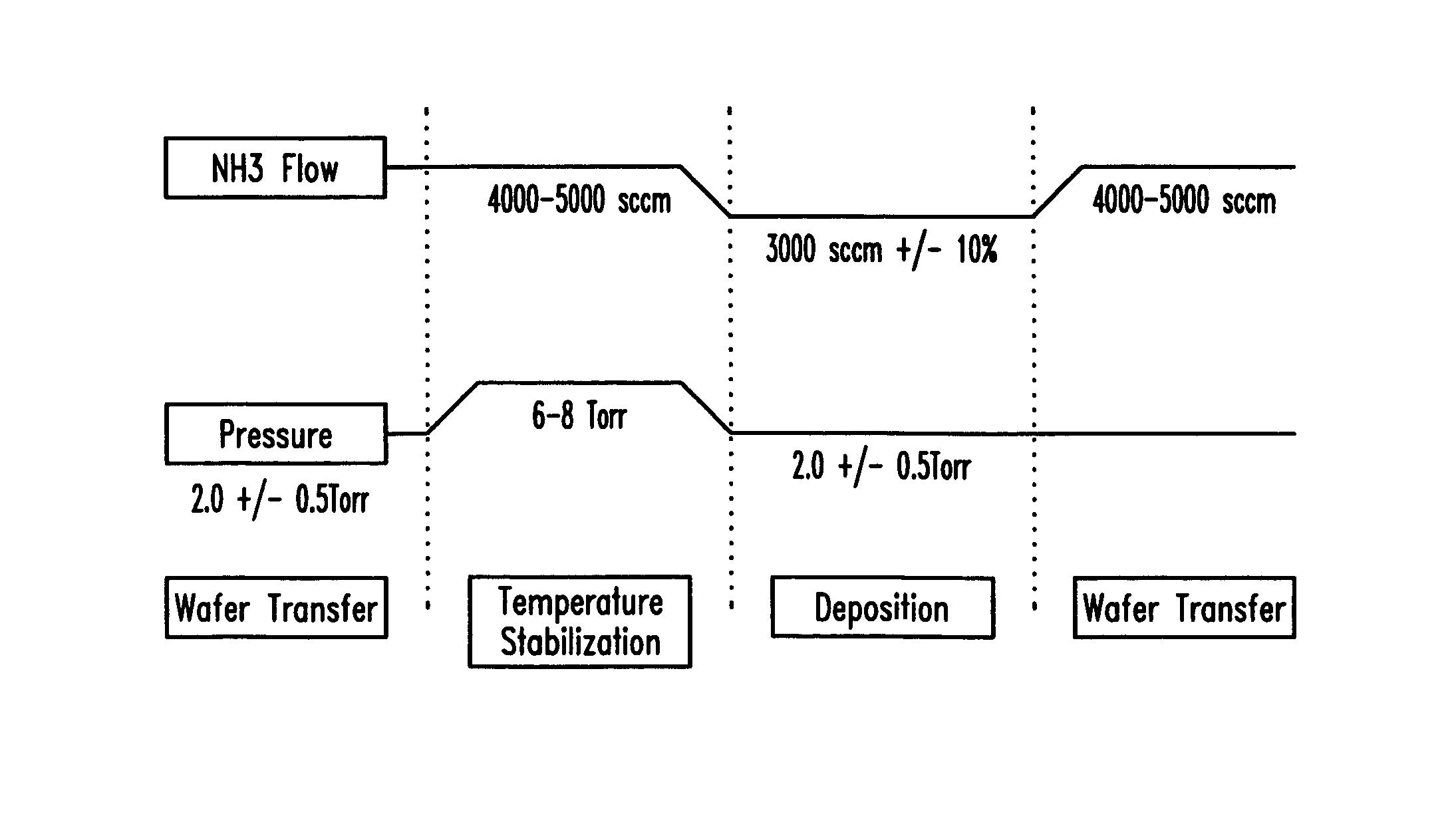
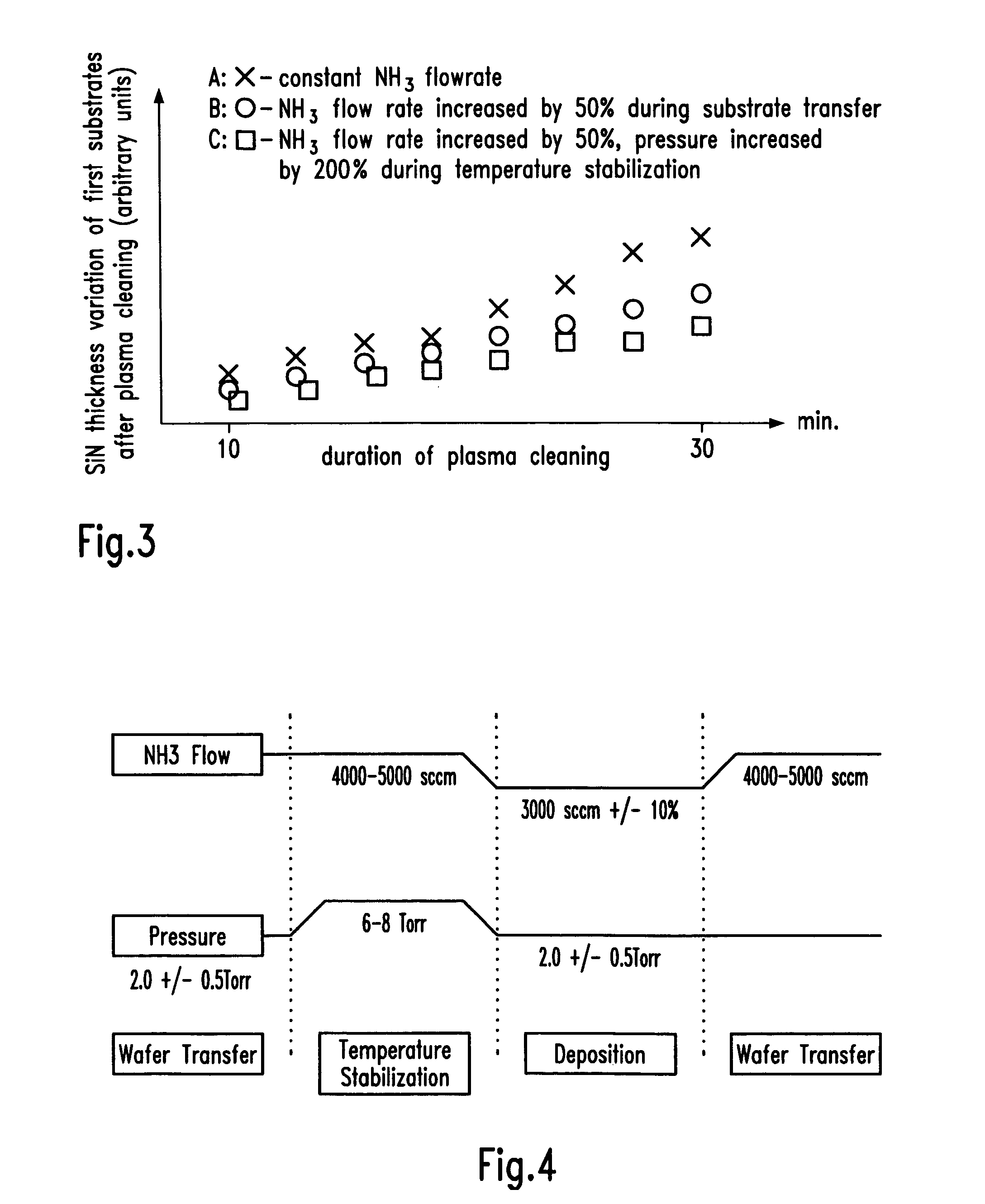
[0011]Generally, the present invention is directed to a method enabling an improved control of process parameters during the deposition of a silicon nitride layer after non-deposition periods of the deposition tool. To this end, the flow rate of the reactant and / or the chamber pressure may be varied prior to the actual deposition step so as to enhance the re-establishment of the process conditions as specified by a given process recipe. As previously explained, the temperature of the substrate and the shower head may be significantly changed upon loading a new substrate into the process chamber or by a preceding operation of the deposition tool in an idle mode or a plasma clean mode. By varying the flow rate of the reactant, which represents the main amount of the gaseous precursors of the deposition process, the shower head's temperature may be rapidly re-adjusted to the specified deposition temperature. Similarly, by correspondingly adapting the chamber pressure at a temperature stabilization phase prior to the actual deposition, a significantly more rapid re-establishment of the actual process parameters may be obtained, thereby improving the substrate-to-substrate thickness uniformity without requiring a plurality of test substrates.

Problems solved by technology

It turns out, however, that silicon nitride thermal CVD processes with temperatures below 600° C. are unavailable and therefore plasma enhanced chemical vapor deposition (PECVD) has become a standard technique for forming silicon nitride layers from the above-specified precursors at temperatures in the range of approximately 200-400° C.
Thus, typically, a plurality of test substrates must be processed prior to the processing of actual product substrates so as to maintain the thickness variation of the silicon nitride layers within specified process margins, thereby reducing productivity and tool utilization.

Method used


Image

  • Method of improving the wafer-to-wafer thickness uniformity of silicon nitride layers
  • Method of improving the wafer-to-wafer thickness uniformity of silicon nitride layers
  • Method of improving the wafer-to-wafer thickness uniformity of silicon nitride layers

Examples


Embodiment Construction

[0021]Illustrative embodiments of the invention are described below. In the interest of clarity, not all features of an actual implementation are described in this specification. It will of course be appreciated that in the development of any such actual embodiment, numerous implementation-specific decisions must be made to achieve the developers' specific goals, such as compliance with system-related and business-related constraints, which will vary from one implementation to another. Moreover, it will be appreciated that such a development effort might be complex and time-consuming, but would nevertheless be a routine undertaking for those of ordinary skill in the art having the benefit of this disclosure.

[0022]The present invention will now be described with reference to the attached figures. Although the various regions and structures of a semiconductor device are depicted in the drawings as having very precise, sharp configurations and profiles, those skilled in the art recogni...


PUM

PropertyMeasurementUnit
pressureaaaaaaaaaa
temperaturesaaaaaaaaaa

Abstract

Wafer-to-wafer thickness uniformity may be improved significantly in a process for depositing a silicon nitride layer in that the flow rate of the reactant and the chamber pressure are varied during a deposition cycle. By correspondingly adapting the flow rate and / or the chamber pressure before and after the actual deposition step, the process conditions may be more effectively stabilized, thereby reducing process variations, even after non-deposition phases of the deposition tool, such as a preceding plasma clean process or an idle period of the tool.

Description

BACKGROUND OF THE INVENTION[0001]1. Field of the Invention[0002]The present invention generally relates to the field of fabricating microstructures, such as integrated circuits, and, more particularly, to the deposition of silicon nitride layers by chemical vapor deposition (CVD).[0003]2. Description of the Related Art[0004]During the fabrication of microstructures, such as integrated circuits, one important process technology is the deposition of dielectric films for various purposes, such as electrically insulating certain device areas, forming a dielectric for capacitors, providing a barrier function against diffusion of undesired materials, creating a desired etch selectivity with respect to other materials, and the like. Especially, in the field of integrated circuit fabrication, a large amount of presently available products is based on silicon, and, hence, the dielectric materials silicon dioxide and silicon nitride are frequently used for the above-identified purposes due to...

Claims


Application Information

Patent Timeline
Patent Type & Authority Patents(United States)
IPC IPC(8): C23C16/00C23C16/34C23C16/44H01L21/318
CPCC23C16/345C23C16/4405H01L21/3185H01L21/02274H01L21/0217
Inventor HUY, KATJARUELKE, HARTMUTTURNER, MICHAEL
Owner GLOBALFOUNDRIES INC
Why Eureka
Try Eureka